Groove MOSFET with terminal voltage-withstanding structure and manufacturing method of groove MOSFET

A voltage-resistant structure and groove technology, which is applied in the manufacture of semiconductor/solid-state devices, semiconductor devices, electrical components, etc., can solve the problems of reduced device reliability life, increased local field strength, and reduced breakdown voltage, etc., to achieve reduction Leakage, improve the lateral withstand voltage, reduce the effect of lateral leakage

Active Publication Date: 2014-05-28
BYD SEMICON CO LTD
View PDF7 Cites 9 Cited by
  • Summary
  • Abstract
  • Description
  • Claims
  • Application Information

AI Technical Summary

Problems solved by technology

However, the problem of increasing the cell density is that the cell size of the current low-voltage trench MOSFET has been reduced to 1um, and the space for further decline is getting smaller and smaller, and the reduction in size will lead to an increase in local field strength, which will inevitably bring Device Reliability Life Reduction
However, if Figure 5 As shown, this process step cannot limit the P-well area and N+ area, and it is impossible to continue to form a P-type annular pressure-resistant ring on the periphery of the chip to improve the withstand voltage and reduce leakage. It is necessary to propose a new terminal design to solve the breakdown The problem of voltage drop and leakage increase

Method used


Image

  • Groove MOSFET with terminal voltage-withstanding structure and manufacturing method of groove MOSFET
  • Groove MOSFET with terminal voltage-withstanding structure and manufacturing method of groove MOSFET
  • Groove MOSFET with terminal voltage-withstanding structure and manufacturing method of groove MOSFET

Examples


Embodiment Construction

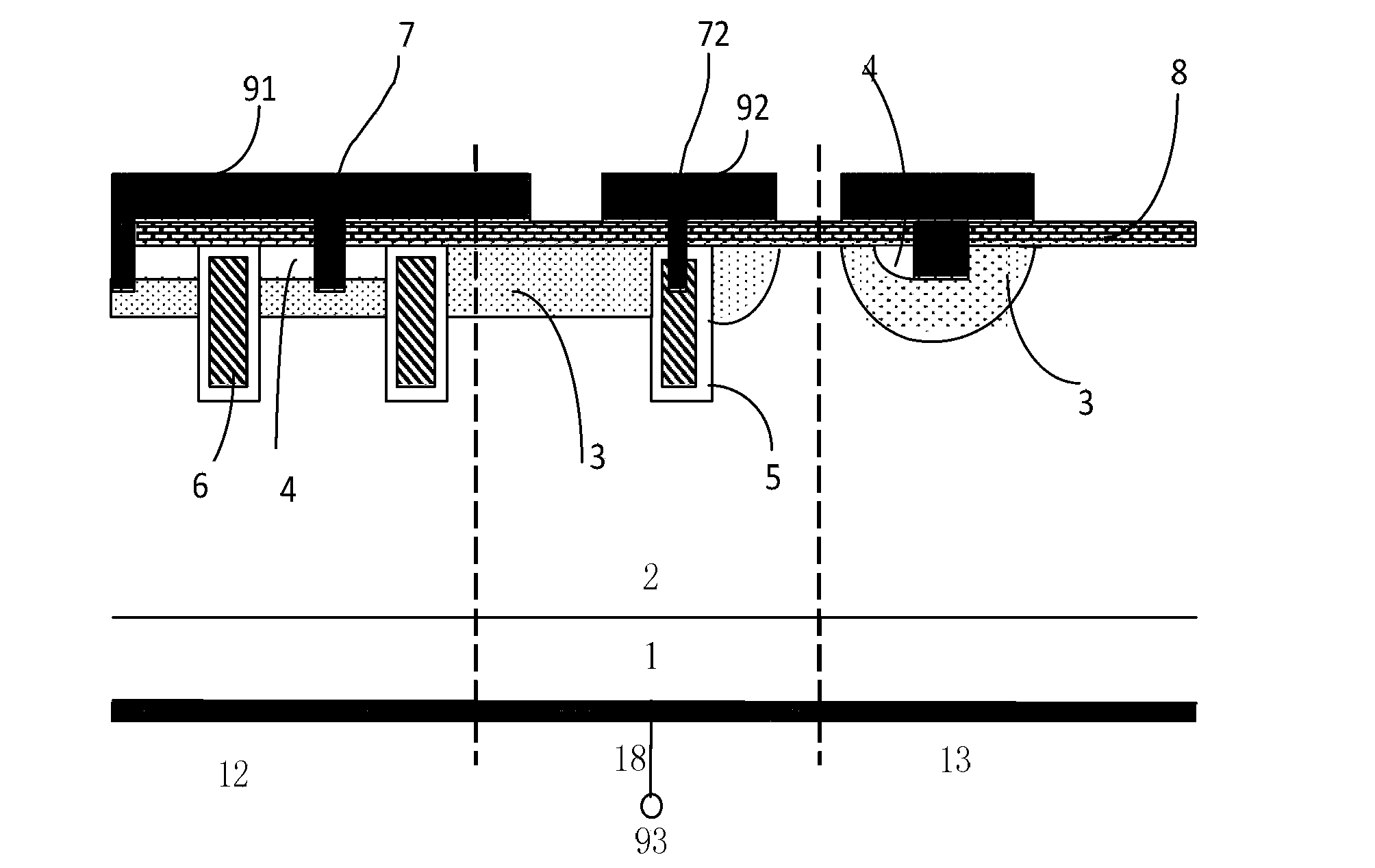
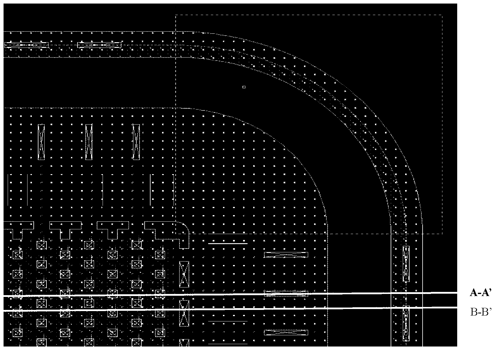
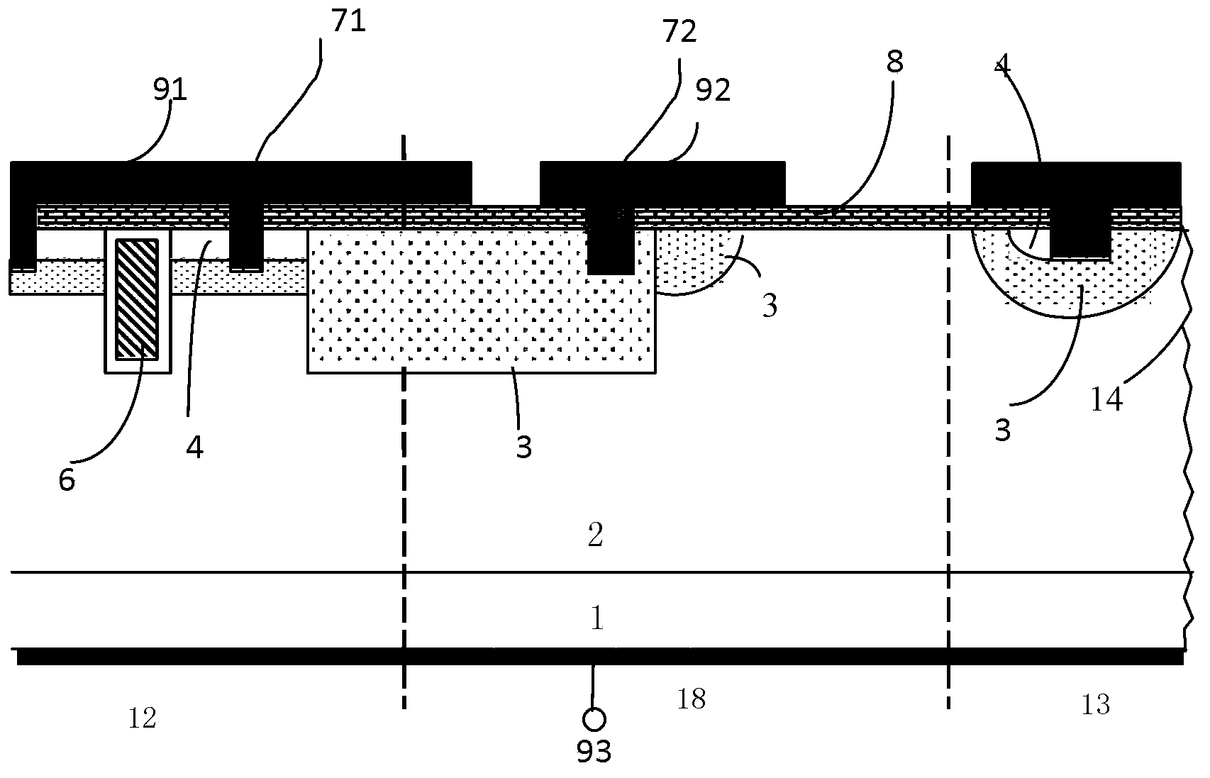
[0045] Embodiments of the present invention are described in detail below, examples of which are shown in the drawings, wherein the same or similar reference numerals designate the same or similar elements or elements having the same or similar functions throughout. The embodiments described below by referring to the figures are exemplary only for explaining the present invention and should not be construed as limiting the present invention.

[0046] In describing the present invention, it should be understood that the terms "longitudinal", "transverse", "upper", "lower", "front", "rear", "left", "right", "vertical", The orientation or positional relationship indicated by "horizontal", "top", "bottom", "inner", "outer", etc. are based on the orientation or positional relationship shown in the drawings, and are only for the convenience of describing the present invention and simplifying the description, rather than Nothing indicating or implying that a referenced device or elem...


PUM


Abstract

The invention brings forward a groove MOSFET with a terminal voltage-withstanding structure and a manufacturing method of the groove MOSFET. Grooves are formed in a cellular area and a terminal area of the groove MOSFET respectively. The grooves of the terminal area are at least two enclosed annular grooves which surround the cellular area. At least one annular groove, which is close to the cellular area, is an isolation ring which is connected with a zero potential. At least one annular groove, which is close to a scribing channel, is a cutoff ring which is connected with the scribing channel. According to the groove MOSFET with the terminal voltage-withstanding structure, the isolation ring is connected with the zero potential so that electric leakage can be effectively inhibited; and the cutoff ring is connected with the scribing channel so that carriers are not accumulated along the cutoff ring, and thus isolation effect and voltage-withstanding effect of the terminal voltage-withstanding structure are enhanced. According to the manufacturing method, voltage-withstanding and electric leakage problems of the groove MOSFET prepared by the three-layer photo-etching technology are solved, transverse electric leakage of the groove MOSFET is reduced, voltage withstanding of devices is enhanced, technology process is simplified and manufacturing cost is lowered without increasing technology complexity.

Description

technical field [0001] The invention belongs to the field of basic electrical components and relates to the preparation of semiconductor devices, in particular to a terminal withstand voltage structure of a trench MOSFET and a manufacturing method thereof. Background technique [0002] Trench MOSFET is a new generation of power semiconductor device that integrates microelectronics technology and power electronics technology. It is widely used in DC- DC converters, voltage regulators, power management modules, automotive electronics and electromechanical control and other fields. [0003] Trench MOSFET was proposed as early as the early 1980s. In the development of trench MOSFET, research on reducing product development costs revolves around obtaining higher cell density, lower on-resistance, more reliable structure and simpler The technological process and other aspects are expanded. [0004] In terms of improving cell density and reducing product cost, with the developmen...

Claims


Application Information

Patent Timeline
Patent Type & Authority Applications(China)
IPC IPC(8): H01L29/78H01L29/06H01L21/336
CPCH01L29/0638H01L29/66666H01L29/7827
Inventor 朱超群钟树理陈宇
Owner BYD SEMICON CO LTD
Why Eureka
Try Eureka