Epitaxial growth method for improving electrostatic endurance capacity of GaN-based light-emitting diode (LED)

An epitaxial growth and static electricity technology, which is applied in crystal growth, single crystal growth, single crystal growth, etc., can solve the problems of device antistatic ability, LED chip leakage, ESD, electrical performance, uneven current distribution, etc., to achieve Effect of Improving ESD Resistance

Active Publication Date: 2014-05-28
宁波安芯美半导体有限公司
View PDF4 Cites 14 Cited by
  • Summary
  • Abstract
  • Description
  • Claims
  • Application Information

AI Technical Summary

Problems solved by technology

However, due to the large lattice mismatch (>11%) and the large difference in thermal expansion coefficient between GaN and sapphire substrate, there are a large number of defects in the GaN epitaxial layer, and the defect density is as high as 1╳10 8 -1╳10 10 cm -2 , these defects appear as linear dislocations in the GaN epitaxial layer and can extend the entire epitaxial layer; some of the linear dislocations will develop into V-type defects after passing through the InGaN/Ga

Method used


Image

  • Epitaxial growth method for improving electrostatic endurance capacity of GaN-based light-emitting diode (LED)
  • Epitaxial growth method for improving electrostatic endurance capacity of GaN-based light-emitting diode (LED)
  • Epitaxial growth method for improving electrostatic endurance capacity of GaN-based light-emitting diode (LED)

Examples


Embodiment 1

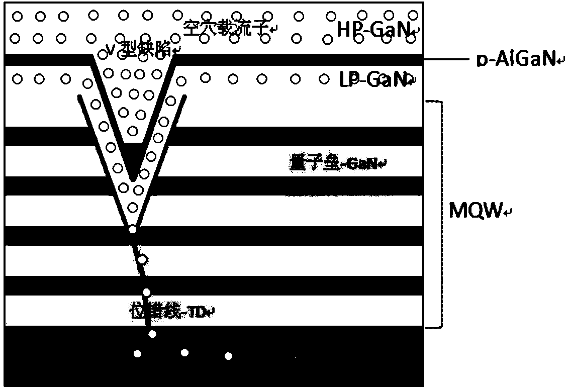
[0028]An epitaxial growth method for improving the electrostatic tolerance of GaN-based LEDs. The LED epitaxial structure includes, from bottom to top, a sapphire substrate, a low-temperature nucleation layer, a high-temperature GaN buffer layer, a high-temperature u-GaN layer, and an n-type GaN layer. layer, shallow quantum well structure SW, low-doped n-GaN electrostatic neutralization layer EN, multi-quantum well light-emitting layer structure MQW, low-temperature p-type GaN layer, p-type AlGaN layer, high-temperature p-type GaN layer, p-type contact layer, Its preparation method comprises the following specific steps:

[0029] (1) Anneal the sapphire substrate in a hydrogen atmosphere, clean the substrate surface at a temperature of 1050°C, and then perform nitriding treatment;

[0030] (2) Lower the temperature to 500°C and grow a 25nm-thick low-temperature GaN nucleation layer with a growth pressure of 400Torr and a molar ratio of V / III of 500;

[0031] (3) After the gr...

Embodiment 2

[0044] An epitaxial growth method for improving the electrostatic tolerance of GaN-based LEDs. The LED epitaxial structure includes, from bottom to top, a sapphire substrate, a low-temperature nucleation layer, a high-temperature GaN buffer layer, a high-temperature u-GaN layer, and an n-type GaN layer. layer, shallow quantum well structure SW, low-doped n-GaN electrostatic neutralization layer EN, multi-quantum well light-emitting layer structure MQW, low-temperature p-type GaN layer, p-type AlGaN layer, high-temperature p-type GaN layer, p-type contact layer, Its preparation method comprises the following specific steps:

[0045] (1) Anneal the sapphire substrate in a hydrogen atmosphere, clean the substrate surface at a temperature of 1150°C, and then perform nitriding treatment;

[0046] (2) Lower the temperature to 620°C, grow a 40nm-thick low-temperature GaN nucleation layer, the growth pressure is 650Torr, and the V / III molar ratio is 3000;

[0047] (3) After the growt...

Embodiment 3

[0060] An epitaxial growth method for improving the electrostatic tolerance of GaN-based LEDs. The LED epitaxial structure includes, from bottom to top, a sapphire substrate, a low-temperature nucleation layer, a high-temperature GaN buffer layer, a high-temperature u-GaN layer, and an n-type GaN layer. layer, shallow quantum well structure SW, low-doped n-GaN electrostatic neutralization layer EN, multi-quantum well light-emitting layer structure MQW, low-temperature p-type GaN layer, p-type AlGaN layer, high-temperature p-type GaN layer, p-type contact layer, Its preparation method comprises the following specific steps:

[0061] (1) Anneal the sapphire substrate in a hydrogen atmosphere, clean the surface of the substrate at a temperature of 1100°C, and then perform nitriding treatment;

[0062] (2) Lower the temperature to 520°C to grow a 30nm-thick low-temperature GaN nucleation layer with a growth pressure of 450Torr and a molar ratio of V / III of 2000;

[0063] (3) Afte...


PUM

PropertyMeasurementUnit
Thicknessaaaaaaaaaa
Thicknessaaaaaaaaaa
Thicknessaaaaaaaaaa

Abstract

The invention provides an epitaxial growth method for improving the electrostatic endurance capacity of a GaN-based light-emitting diode (LED). An LED epitaxial structure sequentially comprises a sapphire substrate, a low-temperature nucleating layer, a high-temperature GaN buffer layer, a high-temperature u-GaN layer, a composite n type GaN layer, a shallow quantum well structure (SW), a low-doped n-GaN electrostatic neutralization layer (EN), a multi-quantum well light-emitting layer structure (MQW), a low-temperature p type GaN layer, a p type Al GaN layer, a high-temperature p type GaN layer and a p type contact layer from bottom to top; the method comprises the steps of (1) inserting an n type Al GaN layer at the 1/3 thickness of the n type GaN layer; (2) inserting the n type GaN layer which is taken as the EN and has the specified thickness and concentration between the SW and the MQW; and (3) inserting the p type Al GaN layer with the specified thickness between the low-temperature p type GaN layer and the high-temperature p type GaN layer. After the epitaxial growth method is adopted, the electronic static discharge (ESD) endurance capacity is effectively improved; a 9mil*9mil chip adopts the conventional epitaxy technique, so that the average ESD stepping value is 200V; and after the epitaxy technique is adopted, the ESD stepping value is obviously increased to 385V.

Description

technical field [0001] The invention relates to the technical field of gallium nitride-based LED preparation, in particular to an epitaxial growth method for improving the electrostatic tolerance of GaN-based LEDs. Background technique [0002] Semiconductor light-emitting diodes (light-emission diodes, LED) are widely used in indicator lights, display screens, backlights and other fields due to their small size, low energy consumption, long life, environmental protection and durability, and LEDs in the field of white lighting Has shown great application potential. With the wide application of LEDs in the field of outdoor display and lighting, the chip itself is required to have more stringent electrostatic tolerance (ESD, Electro Static Discharge). [0003] At present, blue, green, and white LED chips mainly use GaN as the light-emitting matrix material, but due to the lack of GaN single crystal substrates, the GaN epitaxial layer mainly uses sapphire (Al 2 o 3 ) as the ...

Claims


Application Information

Patent Timeline
IPC IPC(8): H01L33/00H01L33/06
CPCC30B29/406H01L33/007H01L33/0095H01L33/025H01L33/06
Inventor 唐军
Owner 宁波安芯美半导体有限公司
Why Eureka
Try Eureka