Method for manufacturing substrate with built-in component and substrate with built-in component using same

A technology with a built-in substrate and a manufacturing method, which is applied in the manufacturing of electrical components, electrical components, printed circuits, etc., can solve problems affecting the formation of conductive vias, connection reliability, insulation, etc., to improve heat resistance and reliability. , the effect of reducing voids

Inactive Publication Date: 2014-05-28
MEIKO ELECTRONICS CO LTD
View PDF5 Cites 0 Cited by
  • Summary
  • Abstract
  • Description
  • Claims
  • Application Information

AI Technical Summary

Problems solved by technology

If there are many such voids, it will affect the formation of conductive vias, connection reliability, or insulation

Method used


Image

  • Method for manufacturing substrate with built-in component and substrate with built-in component using same
  • Method for manufacturing substrate with built-in component and substrate with built-in component using same
  • Method for manufacturing substrate with built-in component and substrate with built-in component using same

Examples


Embodiment Construction

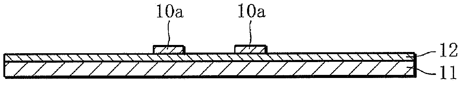
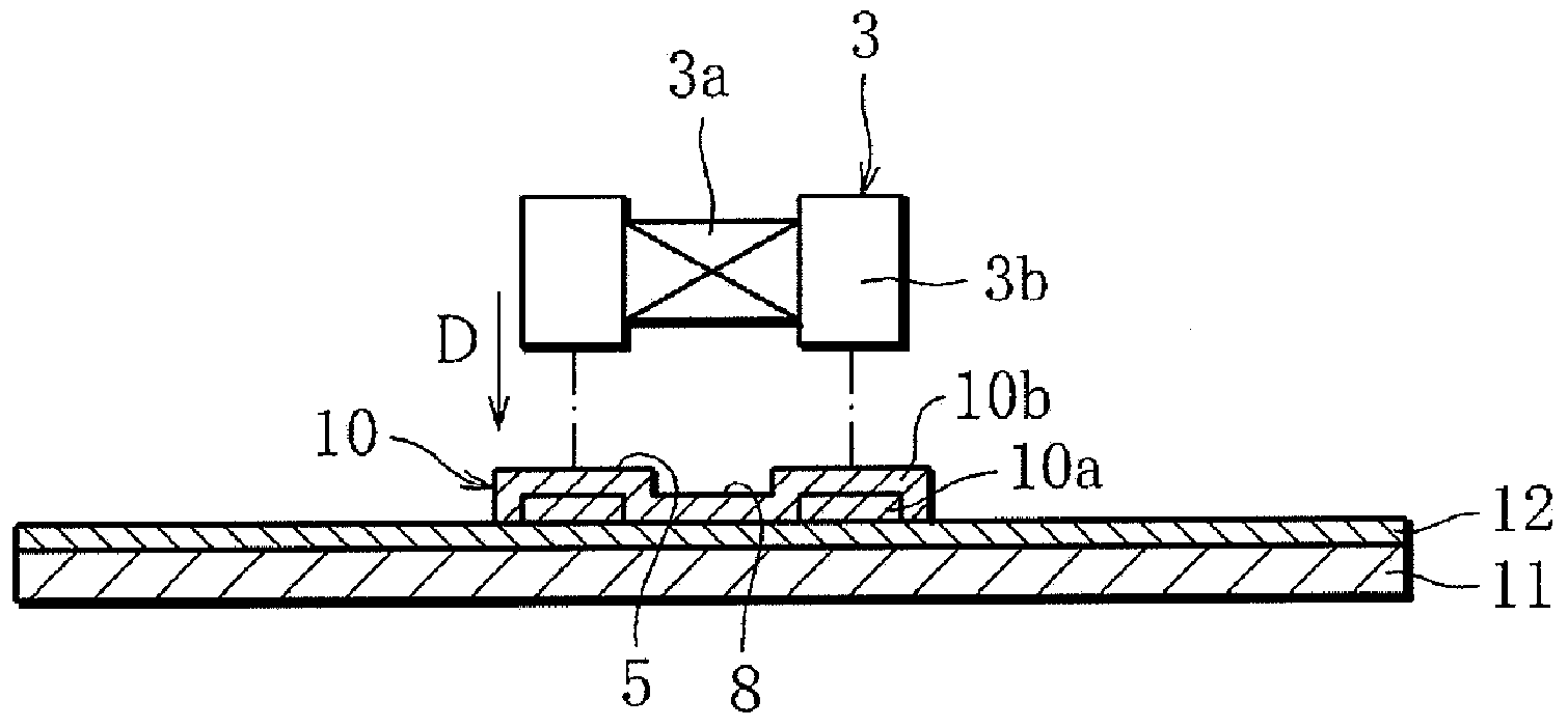
[0041] Such as Figure 1 ~ Figure 3 As shown, the method of manufacturing a component-embedded substrate according to the present invention first performs an adhesive layer forming step. Such as figure 1 As shown, in this step, for example, a member in which the metal layer 12 is formed on the support plate 11 is first prepared. In addition, the support plate 11 has a degree of rigidity required by process conditions. The support plate 11 is formed of a rigid SUS (stainless steel) plate, an aluminum plate, or the like as a support base material. For example, when the support plate 11 is a SUS plate, the metal layer 12 is deposited copper-plated foil of predetermined thickness. Alternatively, when the support plate 11 is an aluminum plate, the metal layer 12 is copper foil pasted on the support plate 11 .

[0042] Then, if figure 2 As shown, the first adhesive body 10 a is coated on the metal layer 12 using, for example, a coater, printing, or the like. Then, after curing ...


PUM


Abstract

This method for manufacturing a substrate with a built-in component includes an adhesive layer forming step in which an adhesive layer (10) is formed on a metal layer (12) formed on a supporting plate (11) and a component mounting step in which an electric or electronic component (3) is mounted on the adhesive layer (10). The component (3) is formed from a component main body (3a) and protruding parts (3b) protruding on the adhesive layer (10) side of the component main body (3a). The adhesive layer (10) formed in the adhesive layer forming step is formed from at least a first and second adhesive body (10a, 10b). The first adhesive body (10a) is formed only in positions corresponding to the protruding parts (3b). The second adhesive body (10b) is formed in a position corresponding to the complete surface of the adhesive layer (10) side of the component (3) after hardening of the first adhesive body (10a). In the component mounting step, the protruding parts (3b) are aligned with the positions of the first adhesive body (10a) and mounted.

Description

technical field [0001] The present invention relates to a manufacturing method of a component-embedded substrate and a component-embedded substrate using the manufacturing method. Background technique [0002] There are various methods of manufacturing component-embedded substrates (for example, refer to Patent Document 1). In this method, an adhesive layer is formed on copper foil using a coater or a printing process, components to be embedded are mounted on the adhesive layer, and the adhesive layer is cured to fix the components. Then, the components are embedded in the insulating base material by lamination and lamination, and via holes reaching the terminals of the components from the outside are formed by laser processing. Then, a plating process is performed on the via hole so as to be used as a conductive via hole to realize electrical connection with the terminal. [0003] However, the above method may generate voids (voids) inside the adhesive layer. This void e...

Claims


Application Information

Patent Timeline
Patent Type & Authority Applications(China)
IPC IPC(8): H05K3/46H05K3/28
CPCH05K5/065H05K2201/10431H05K13/046H05K1/185H05K1/188H05K2203/06H05K2201/10636H05K3/4602Y10T156/1057Y10T156/10Y02P70/50
Inventor 松本徹户田光昭今村圭男
Owner MEIKO ELECTRONICS CO LTD
Why Eureka
Try Eureka