Method for processing micro-electromechanical systems (MEMS) sensor

A processing method and sensor technology, which are applied in the process of producing decorative surface effects, metal material coating process, decorative arts, etc., can solve the problems of high control difficulty, high cost, complex process, etc. The effect of low production cost and simple process

Active Publication Date: 2014-06-04
ADVANCED SEMICON MFG CO LTD
View PDF5 Cites 10 Cited by
  • Summary
  • Abstract
  • Description
  • Claims
  • Application Information

AI Technical Summary

Problems solved by technology

[0004] The film or backplane of the MEMS microphone usually chooses one of the following three: 1. Composite layer, the process is relatively complicated and the control is difficult; 2. Single-layer polysilicon, the polysilico

Method used


Image

  • Method for processing micro-electromechanical systems (MEMS) sensor
  • Method for processing micro-electromechanical systems (MEMS) sensor
  • Method for processing micro-electromechanical systems (MEMS) sensor

Examples


Example Embodiment

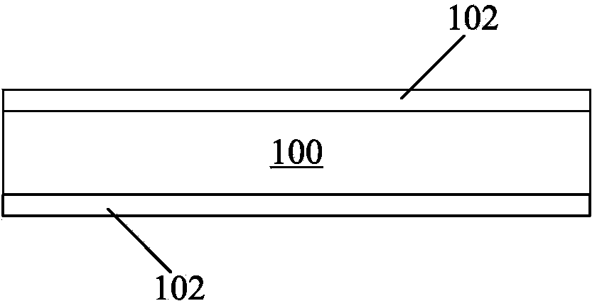
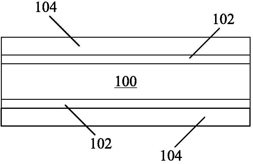
[0033] The invention is mainly used for the processing of micro sensors such as MEMS microphones, and mainly involves key processes such as low-stress thin film technology, deep groove etching technology, special photoresist protection technology after deep groove etching, structure release and drying. The invention does not require thinning of silicon wafers, and ensures smooth tape-out and achieves good yield through special film stress control technology.

[0034] The present invention will be further described below with reference to specific embodiments and accompanying drawings. More details are set forth in the following description to facilitate a full understanding of the present invention, but it is obvious that the present invention can be implemented in many other ways that are different from those described herein. Those skilled in the art can make similar promotion and deduction according to the actual application situation without violating the connotation of the...


PUM


Abstract

The invention provides a method for processing a micro-electromechanical systems (MEMS) sensor. The method comprises the following steps: providing a silicon substrate, and sequentially forming an etching barrier layer and a first electrode layer on the positive and reverse sides of the silicon substrate; patterning the first electrode layer on the positive side of the substrate; respectively and sequentially forming a sacrificial layer and a second electrode layer on the substrate; patterning the second electrode layer on the positive side of the substrate; etching the sacrificial layer to form a contact hole through the patterned second electrode layer, and respectively forming metal contact at the bottom of the contact hole and the second electrode layer; sequentially etching the second electrode layer, the sacrificial layer, the first electrode layer and the etching barrier layer from the reverse side of the substrate, continuously etching the substrate so as to reach the etching barrier layer on the positive side and stopping, and forming a deep groove with a downward opening; coating photoresist above the front side of the substrate to protect, and reserving a subsequent area in which the sacrificial layer needs to be etched; and etching the sacrificial layer through the patterned second electrode layer, and removing the etching barrier layer at the bottom of the deep groove. According to the method, the process steps are simplified, a smooth flow is guaranteed, and high yield is realized.

Description

technical field [0001] The invention relates to the technical field of micro-electromechanical systems (MEMS) manufacturing, in particular, the invention relates to a method for processing MEMS sensors. Background technique [0002] The MEMS microphones currently on the market are usually condenser microphones, the main structure of which is a movable membrane and an almost motionless backplane. The two electrodes forming the capacitor may be polycrystalline silicon, single crystal silicon, a composite layer of polycrystalline silicon plus silicon nitride, a composite layer of silicon nitride and metal, and the like. When the sound pressure acts on the film, the film will be displaced in different degrees according to the intensity of the sound pressure, which will cause the change of the capacitance, and the corresponding output voltage will change, and the corresponding sound signal can be read out through the amplifying circuit. [0003] MEMS microphones are usually prod...

Claims


Application Information

Patent Timeline
IPC IPC(8): B81C1/00
Inventor 颜毅林徐元俊戴竝盈孙钧刘伟
Owner ADVANCED SEMICON MFG CO LTD
Why Eureka
Try Eureka