Low-temperature polycrystalline silicon thin film transistor, array substrate and manufacturing method of array substrate

A thin-film transistor, low-temperature polysilicon technology, applied in transistors, semiconductor/solid-state device manufacturing, electrical solid-state devices, etc., can solve the problems of unsuitable thin-film transistors and high temperature, avoid related defects and undesirable phenomena, improve performance, and simplify production. The effect of craftsmanship

Inactive Publication Date: 2014-06-04
BOE TECH GRP CO LTD
View PDF4 Cites 18 Cited by
  • Summary
  • Abstract
  • Description
  • Claims
  • Application Information

AI Technical Summary

Problems solved by technology

The existing technology adopts thermal annealing process with high temperature,

Method used


Image

  • Low-temperature polycrystalline silicon thin film transistor, array substrate and manufacturing method of array substrate
  • Low-temperature polycrystalline silicon thin film transistor, array substrate and manufacturing method of array substrate
  • Low-temperature polycrystalline silicon thin film transistor, array substrate and manufacturing method of array substrate

Examples


Embodiment Construction

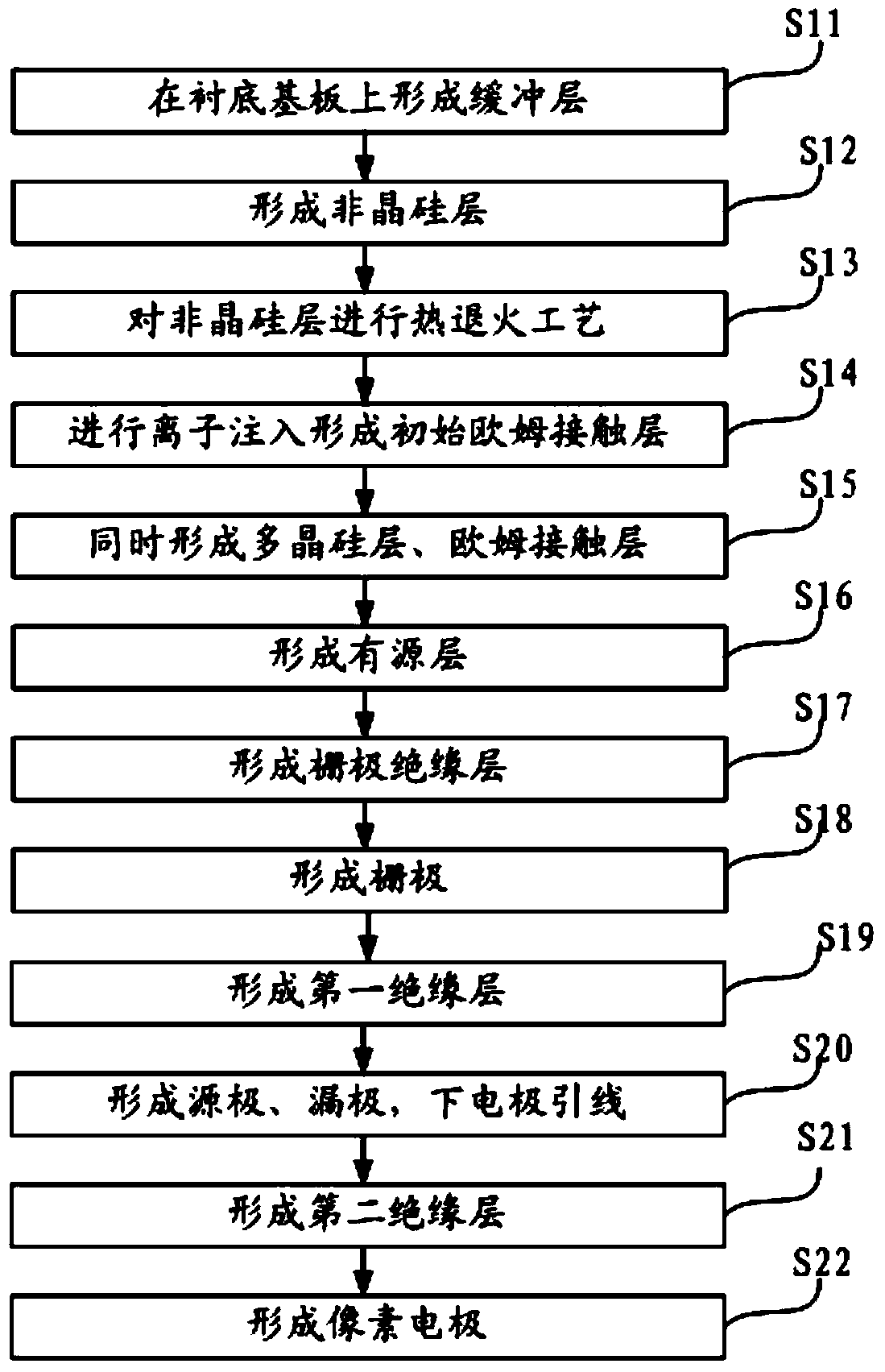
[0037] Embodiments of the present invention provide a low temperature polysilicon thin film transistor, an array substrate and a manufacturing method thereof, which are used to simplify the manufacturing process of the low temperature polysilicon thin film transistor and improve the performance of the low temperature polysilicon thin film transistor.

[0038] In the manufacturing method of the low-temperature polysilicon thin film transistor provided by the embodiment of the present invention, before the polysilicon layer is formed from the amorphous silicon layer, the amorphous silicon is ion-implanted to form an initial ohmic contact layer, and the polysilicon layer is formed from the amorphous silicon layer at the same time. Forming an ion-activated ohmic contact layer simplifies the manufacturing process.

[0039] The ohmic contact layer of the present invention is also called source-drain doped layer, and the ohmic contact layer includes two mutually independent regions, w...


PUM


Abstract

The invention discloses a low-temperature polycrystalline silicon thin film transistor, an array substrate and a manufacturing method of the array substrate, so that manufacturing process procedures of the thin film transistor are simplified. The method includes the process that an active layer and an ohmic contact layer are formed on a substrate. The process that the active layer and the ohmic contact layer are formed on the substrate specifically includes the steps of forming an amorphous silicon layer on the substrate through; injecting impurity ions into at least the area of an ohmic contact layer to be formed of the amorphous silicon layer by means of an ion implantation method, wherein the area of the ohmic contact layer to be formed forms an initial ohmic contact layer; carrying out the excimer laser annealing process on the amorphous silicon layer after the impurity ion implantation technology; crystallizing the amorphous silicon layer after the excimer laser annealing process to form a polycrystalline silicon layer, and forming a final ohmic contact layer through the initial ohmic contact layer; carrying out the composition process on the polycrystalline silicon layer after the excimer laser annealing process to form the active layer.

Description

technical field [0001] The invention relates to the field of manufacturing thin film transistors, in particular to a low-temperature polysilicon thin film transistor, an array substrate and a manufacturing method thereof. Background technique [0002] In pixel units of various display devices, a thin film transistor (Thin Film Transistor, TFT) that drives the display device by applying a driving voltage is widely used. Amorphous silicon (a-Si) materials with better stability and processability have been used in the active layer of TFTs, but the carrier mobility of a-Si materials is low, which cannot meet the needs of large-scale, high-resolution display devices requirements, especially the requirements of the next generation of active matrix organic light emitting display devices (Active Matrix Organic Light Emitting Device, AMOLED). Compared with amorphous silicon (a-Si) thin film transistors, polysilicon, especially low-temperature polysilicon thin film transistors have h...

Claims


Application Information

Patent Timeline
IPC IPC(8): H01L21/336H01L21/28H01L21/84H01L29/786H01L29/45H01L27/12
CPCH01L27/1222H01L27/1255H01L27/1259H01L29/456H01L29/66757H01L29/78675H01L27/1274H01L21/02422H01L21/02488H01L21/0262H01L28/60H01L27/1285H01L21/02532H01L21/02686H01L21/268H01L21/02592H01L21/28512H01L21/324H01L27/1218H01L27/1262H01L28/40
Inventor 毛雪
Owner BOE TECH GRP CO LTD
Why Eureka
Try Eureka