
Display device

A technology for display devices and hydrogen barrier layers, applied in lighting devices, electroluminescent light sources, electric light sources, etc., can solve the problems of initial characteristics and long-term reliability degradation of thin film transistors

Active Publication Date: 2014-06-04
SAMSUNG DISPLAY CO LTD
View PDF4 Cites 15 Cited by
  • Summary
  • Abstract
  • Description
  • Claims
  • Application Information

AI Technical Summary

Problems solved by technology

Hydrogen contained in the gas flows through the active layer, thus deteriorating the initial characteristics and long-term reliability of the thin film transistor

Method used


Image

  • Display device
  • Display device
  • Display device

Examples


Embodiment Construction

[0033] Hereinafter, the content of the invention will be described in more detail with reference to the accompanying drawings, in which exemplary embodiments of the content of the invention are shown. However, this matter may be embodied in many different forms without departing from the spirit or scope of embodiments of the present invention.

[0034] Throughout the specification, unless expressly stated to the contrary, the term "comprise" and variations such as "comprises" or "comprising" should be understood to mean encompassing the stated elements. Furthermore, in the specification, it will be understood that when an element such as a layer, film, region, or substrate is referred to as being "on" another element, it can be directly on the other element or intervening elements may also be present. Also, in the specification, the term "on" means located on or below the target portion, for example, as described in the drawings, and does not necessarily mean on the upper side...


PUM


Abstract

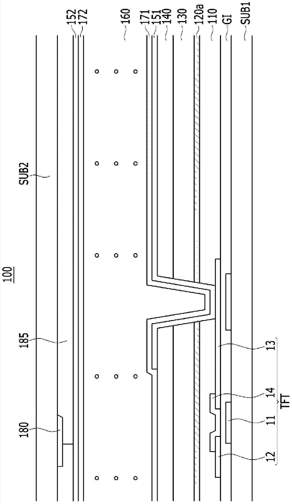
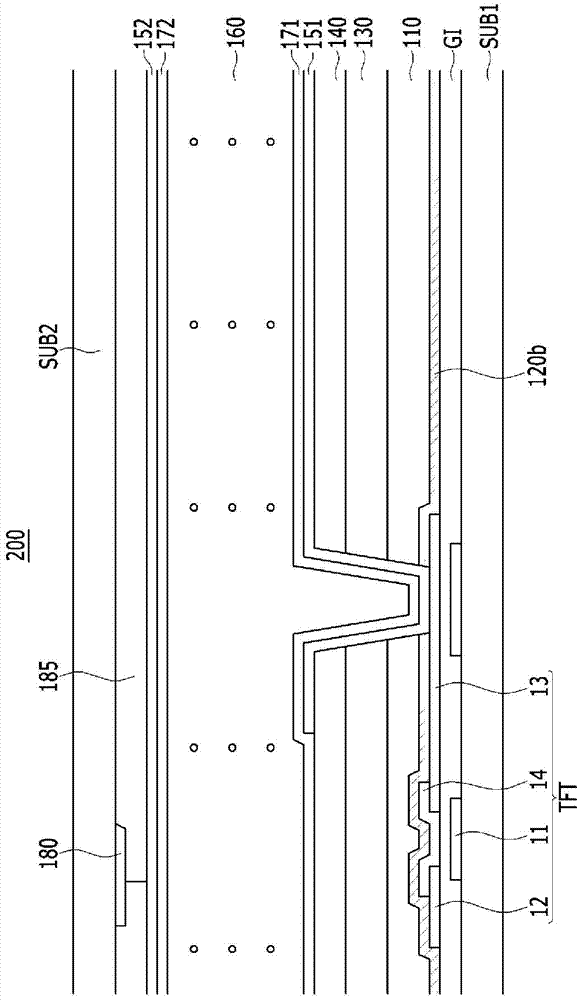
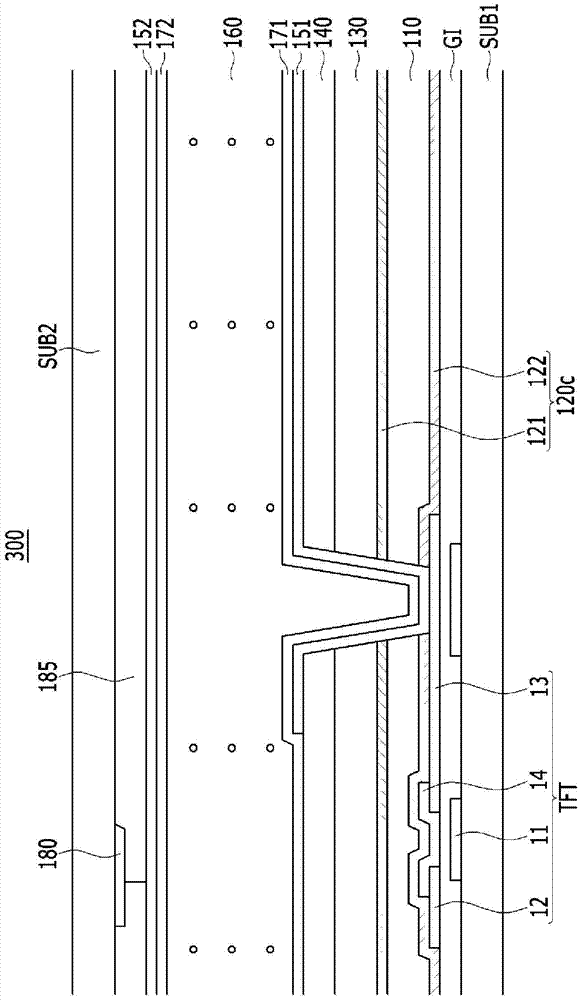
In an aspect, a display device including: a substrate; a thin film transistor formed on the substrate, and comprising an active layer formed of an oxide semiconductor; a passivation layer formed on the thin film transistor; and a hydrogen blocking layer positioned between the active layer and the passivation layer is provided.

Description

technical field [0001] The described technology relates generally to a display device, and more specifically, to a display device including a thin film transistor using an oxide semiconductor as an active layer. Background technique [0002] Thin film transistors can be used as pixel switching elements in flat panel displays. The active layer of the thin film transistor may be mainly formed of amorphous silicon or polysilicon. Amorphous silicon active layers can be easily deposited over large areas and processed at low temperatures, but suffer from low charge mobility. The polysilicon active layer has excellent electrical characteristics due to high charge mobility, but requires high temperature processing and has difficulty in reliable uniformity. [0003] A thin film transistor including an oxide semiconductor such as zinc oxide or gallium-indium-zinc oxide as an active layer has both the advantage of being able to process at low temperature of amorphous silicon and the ...

Claims


Application Information

Patent Timeline
IPC IPC(8): H01L27/32H01L51/52H05B44/00
CPCH01L27/3272H01L27/3258H01L29/7869H01L27/3244H01L27/1225H10K59/124H10K59/126H01L27/1248H01L29/78606H10K59/12
Inventor 金正晥金庚宪尹柱善
Owner SAMSUNG DISPLAY CO LTD
Learn More