Double-gate graphene transistor with aluminum oxide as gate dielectric and manufacturing method thereof

An aluminum oxide and transistor technology, applied in the field of microelectronics, can solve the problems of growth, can not play an insulating role, affect device performance, etc., and achieve the effects of improving modulation effect, suppressing scattering effect, and simplifying manufacturing process

Active Publication Date: 2014-06-04
XIDIAN UNIV
View PDF5 Cites 5 Cited by
  • Summary
  • Abstract
  • Description
  • Claims
  • Application Information

AI Technical Summary

Benefits of technology

This patented technology solves issues such as leaks caused by defective semiconductor layers or poor crystal quality during growth of graphite films for use in electronic components like capacitors (C). By growing an epitaxial layer onto a special type of material called graphene instead of forming another thin film), this new method allows for greater flexibility in design while maintaining good performance characteristics over time. Additionally, the addition of graphene also enhances certain properties such as reducing resistance between different parts of circuitry. Overall, these technical improvements improve the efficiency and lifespan of electronic component designs made from this novel technique compared to previous methods.

Problems solved by technology

This patents discuss how graphite (graphen) exhibits unique physical features like excellent conductivity, transparency, thermal conduction, small size, ability to form thin films, and potential applications in fields related industries including semiconductor technology. These technical problem addressed in this patented paper includes improving the quality and efficiency of graphitics while reducing their impact on other components within electronic systems.

Method used


Image

  • Double-gate graphene transistor with aluminum oxide as gate dielectric and manufacturing method thereof
  • Double-gate graphene transistor with aluminum oxide as gate dielectric and manufacturing method thereof
  • Double-gate graphene transistor with aluminum oxide as gate dielectric and manufacturing method thereof

Examples


Embodiment 1

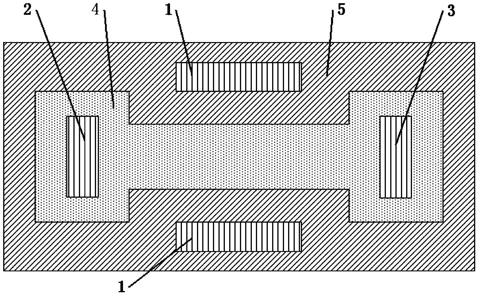
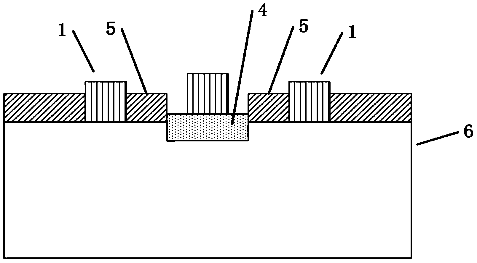
[0038] Step 1: Wash the 6H-SiC sample to remove surface contaminants such as Figure 4 (a).

[0039] (1.1) Use NH for 6H-SiC samples 4 OH+H 2 o 2 Soak the sample in the reagent for 10 minutes, take it out and dry it to remove the organic residue on the surface of the sample;

[0040] (1.2) Use HCl+H on the 6H-SiC sample after removing the surface organic residues 2 o 2 The reagent soaked the sample for 10 minutes, took it out and dried it to remove ionic contamination.

[0041] Step 2: Deposit a layer of Al on the surface of the 6H-SiC sample 2 o 3 ,like Figure 4 (b).

[0042] (2.1) Put the SiC sample into the growth chamber, and flow N into the growth chamber with a flow rate of 10 sccm 2 Perform a 2-minute purge and repeat the cycle 5 times;

[0043] (2.2) Turn on the thermostat, heat the growth chamber to 250°C, and heat the gas path to 40°C for 60 minutes;

[0044] (2.3) Introduce N with a flow rate of 10 sccm into the growth chamber 2 A 2 min purge was perfo...

Embodiment 2

[0072] Step 1: Clean the 4H-SiC sample to remove surface contaminants such as Figure 4 (a).

[0073] Use NH for 4H-SiC samples 4 OH+H 2 o 2 Soak the sample in the reagent for 10 minutes, take it out and dry it to remove the organic residue on the surface of the sample; use HCl+H 2 o 2 The reagent soaked the sample for 10 minutes, took it out and dried it to remove ionic contamination.

[0074] Step 2: Deposit a layer of Al on the surface of the 4H-SiC sample 2 o 3 ,like Figure 4 (b).

[0075] 2a) Put the SiC sample into the growth chamber, and flow 10 sccm of N into the growth chamber 2 Perform a 2-minute purge and repeat the cycle 5 times;

[0076] 2b) Turn on the thermostat, heat the growth chamber to 250°C, and heat the gas path to 40°C for 60 minutes;

[0077] 2c) Flow 10 sccm of N into the growth chamber 2 A 2 min purge was performed and the cycle was repeated 3 times. Thereafter, the flow rate of 15 sccm of N was continuously passed into the growth chamber...

Embodiment 3

[0095] Step A: Use NH on the 4H-SiC substrate substrate 4 OH+H 2 o 2 Soak the sample in the reagent for 10 minutes, take it out and dry it to remove the organic residue on the surface of the sample; use HCl+H 2 o 2 Soak the sample in the reagent for 10 minutes, take it out and dry it to remove ionic contaminants such as Figure 4 (a).

[0096] Step B: Deposit a layer of Al on the surface of the 4H-SiC sample 2 o 3 film, such as Figure 4 (b)

[0097] B1) Put the SiC sample into the growth chamber, and flow 10 sccm of N into the growth chamber 2 Perform a 2-minute purge and repeat the cycle 5 times;

[0098] B2) Turn on the thermostat, heat the growth chamber to 250°C, and heat the air circuit to 40°C for 60 minutes;

[0099] B3) Infuse N with a flow rate of 10 sccm into the growth chamber 2 Carry out the purging of 2 minutes, repeat cycle 3 times, thereafter, feed the N that the flow rate is 15 sccm continuously to the growth chamber 2 ;

[0100] B4) Introduce wat...


PUM

PropertyMeasurementUnit
Thicknessaaaaaaaaaa
Lengthaaaaaaaaaa
Widthaaaaaaaaaa

Abstract

The invention discloses a double-gate graphene transistor with aluminum oxide as gate dielectric and a manufacturing method thereof. The double-gate graphene transistor with the aluminum oxide as the gate dielectric mainly solves the problems of reduction of carrier mobility and carrier scattering in a graphene channel due to top grate dielectric of a graphene transistor in the manufacturing process in the prior art. The double-gate graphene transistor is structurally characterized in that two gate electrodes are arranged on the two sides of the graphene channel respectively to form a double-gate structure. The manufacturing method includes the first step of depositing a layer of aluminum oxide on the surface of a washed silicon carbide sample wafer and etching out a structural graph on the aluminum oxide layer, the second step of placing the etched sample wafer into a quartz tube, feeding carbon tetrachloride to react with silicon carbide to generate a carbon film, then placing the sample wafer into argon to carry out annealing to generate graphene and carrying out etching on the portions, 60-400 nanometers away from the two sides of the graphene channel, of the aluminum oxide layer to form gate grooves, and the third step of depositing metal on the sample wafer and etching the sample wafer to form a metal contact layer of the transistor. The double-gate graphene transistor manufactured through the method is capable of effectively improving the carrier mobility ratio and the modulation capacity of the gate electrodes on the channel current.

Description


Claims


Application Information

Patent Timeline
Owner XIDIAN UNIV
Why Eureka
Try Eureka