
Schottky clamping diode with groove structure and terminal structure

A terminal structure and diode technology, applied in the field of electronics, can solve problems such as concentration, large voltage drop of oxide layer structure, weak withstand voltage, etc.

Inactive Publication Date: 2014-06-11
SHANGHAI HUAHONG GRACE SEMICON MFG CORP
View PDF5 Cites 2 Cited by
  • Summary
  • Abstract
  • Description
  • Claims
  • Application Information

AI Technical Summary

Problems solved by technology

[0004] However, due to the existence of the trench, the electric field will be concentrated at the bottom of the trench, resulting in a relatively weak withstand voltage at this position, and at the same time, the oxide layer structure at this position needs to withstand a large voltage drop

Method used


Image

  • Schottky clamping diode with groove structure and terminal structure
  • Schottky clamping diode with groove structure and terminal structure
  • Schottky clamping diode with groove structure and terminal structure

Examples


Embodiment Construction

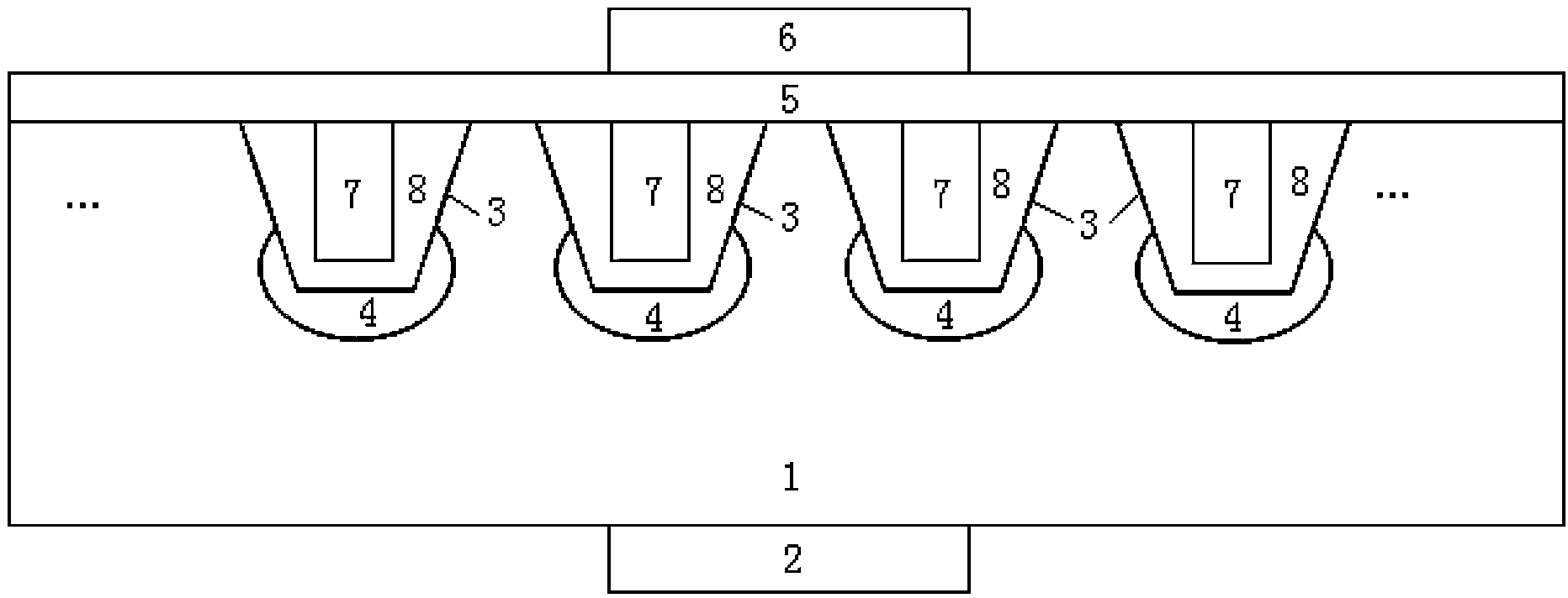
[0020] see image 3 As shown, in the following embodiments, taking N-type epitaxy as an example, the improved Schottky clamp diode with trench structure includes:

[0021] An N-type epitaxial layer 1 is used as the cathode 2 of the Schottky embedded diode with trench structure. The resistivity and thickness of the N-type epitaxial layer 1 are determined according to the reverse withstand voltage of the product itself.

[0022] A plurality of trenches 3 formed by an etching process in the N-type epitaxial layer 1 first grow a layer of first oxide layer 8 inside the trenches 3, and then fill them by thermal oxidation or CVD (chemical vapor deposition) Into the polysilicon 7, and finally form the trench region.

[0023] A P-type doped region (P well) 4 formed by ion implantation at the bottom of the trench 3, the P-type doped region 4 wraps the bottom of the trench 3, and each P-type doped region 4 is mutually will not be connected.

[0024] The metal layer 5 formed on the up...


PUM


Abstract

The invention discloses a Schottky clamping diode with a groove structure. The diode comprises an N-type epitaxial layer serving as the negative electrode of the Schottky clamping diode with the groove structure, multiple grooves formed in the N-type epitaxial layer, P-type doping areas formed on the bottom of each groove, and a metal layer formed at the upper end of the N-type epitaxial layer and at the upper end of a groove area, wherein an oxidation layer is formed in each groove, polycrystalline silicon is arranged above each oxidation layer to enable the corresponding groove to be filled up, the multiple grooves and the oxidation layers and polycrystalline silicon inside form the groove area, the bottom of each groove is wrapped in the corresponding P-type doping area, the P-type doping areas are not mutually connected, and the N-type epitaxial layer and the groove area are connected through the metal layer to serve as the positive electrode of the Schottky clamping diode with the groove structure. The invention further discloses a terminal structure matched with the Schottky clamping diode with the groove structure. According to the Schottky clamping diode with the groove structure and the terminal structure, the pressure resistance of the bottom of each groove can be improved, so that reverse pressure resistance of products is improved.

Description

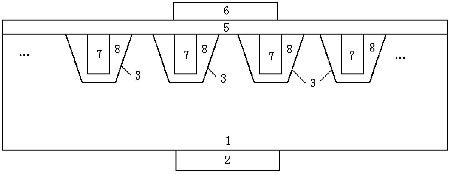
technical field [0001] The invention relates to the field of electronic technology, in particular to a Schottky embedded diode with a trench structure. The invention also relates to a terminal structure matched with the trench-containing Schottky embedded diode. Background technique [0002] Schottky embedded diodes occupy a place in the field of power devices due to their good forward conduction characteristics and fast switching speed, but due to the use of metal-semiconductor contacts in their production, their reverse withstand voltage and reverse leakage conditions are not good. [0003] In 1990, a product called TMBS (Schottky embedded diode with trench structure) was proposed (see figure 2 shown), the traditional Schottky clamp diode (SBD, see figure 1 As shown) the reverse breakdown point is moved from the silicon surface to the bottom of the groove in the body. In this way, the reverse breakdown voltage BV of SBD products can be made higher while ensuring a small...

Claims


Application Information

Patent Timeline
IPC IPC(8): H01L29/872H01L29/06
CPCH01L29/8725H01L29/47
Inventor 刘远良衷世雄
Owner SHANGHAI HUAHONG GRACE SEMICON MFG CORP
Learn More