Single-layer membrane loading type four-layer substrate micro-strip-micro-strip connecting structure

An interconnection structure and single-layer film technology, which is applied in the direction of connection devices, electrical components, circuits, etc., can solve problems that affect circuit performance and complex interconnection structures

Active Publication Date: 2014-06-18
UNIV OF ELECTRONIC SCI & TECH OF CHINA
View PDF5 Cites 4 Cited by
  • Summary
  • Abstract
  • Description
  • Claims
  • Application Information

AI Technical Summary

Problems solved by technology

[0003] For the existing technology, when realizing the multilayer circuit technology, LTCC (low temperature co-fired ceramic technology) is often used. The interconnection structure based on LTCC technology is generally more complicated,

Method used


Image

  • Single-layer membrane loading type four-layer substrate micro-strip-micro-strip connecting structure
  • Single-layer membrane loading type four-layer substrate micro-strip-micro-strip connecting structure
  • Single-layer membrane loading type four-layer substrate micro-strip-micro-strip connecting structure

Examples


Embodiment Construction

[0045] Below in conjunction with accompanying drawing, the present invention is further explained:

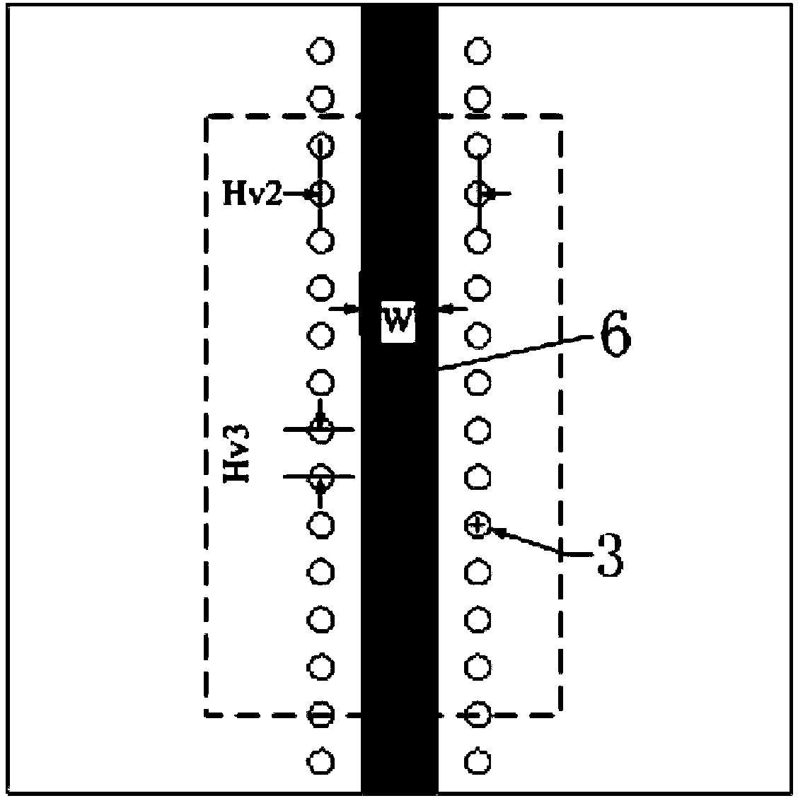
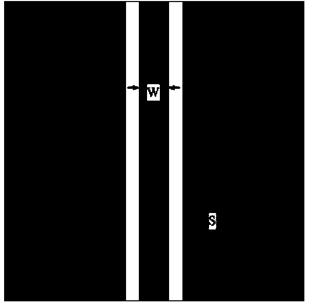
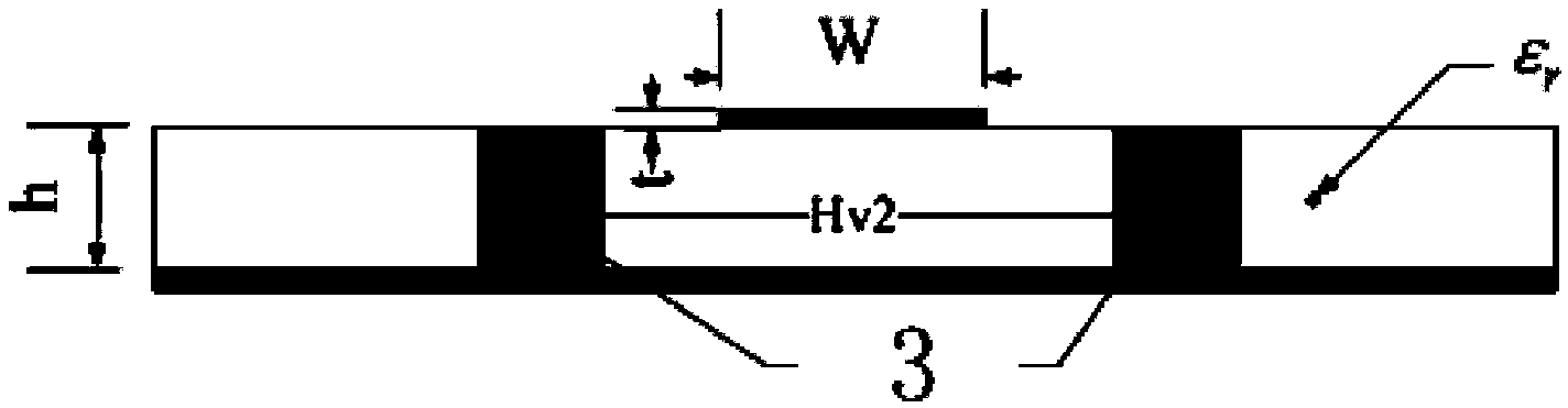
[0046] Firstly, design the quasi-grounded coplanar waveguide according to the general design method of the grounded coplanar waveguide, such as Figure 1a Shown is the top view of the ground-like coplanar waveguide, the center is the microstrip line 6, the line width is W, the two sides of the microstrip line are metal vias, and the distance between the two metal vias 3 is Hv2, and its structure can be equivalent For such Figure 1b A grounded coplanar waveguide is shown, where W is the line width and S is the clearance from the ground plane. Figure 2 is a cross-sectional view of a quasi-grounded coplanar waveguide and a coplanar waveguide structure. When using a grounded coplanar waveguide equivalent to a quasi-grounded coplanar waveguide structure: Hv2=W+2S

[0047] Using the design formula of grounded coplanar waveguide, when The characteristic impedance Z of the side wal...


PUM


Abstract

Provided is a single-layer membrane loading type four-layer substrate micro-strip-micro-strip connecting structure. Low-reflection and low-loss transmission of microwave signals between layers in a four-layer medium substrate is achieved. The structure comprises four medium layers, a metal layer is arranged between every two medium layers, micro-strip wires are arranged on a first medium layer at the top layer and a fourth medium layer at the bottom layer, and the micro-strip wires are connected with signal through holes of the metal layers by penetrating through the medium layers vertically. Metal through hole columns are evenly distributed in the two sides of each micro-strip wire. Metal through holes are formed around the signal through holes according to a circular array in a distributing mode. The structure is characterized in that metal hole reverse welding discs are arranged at the positions where the signal through holes penetrate through the metal layers, the circular centers of the metal hole reverse welding discs are on the center lines of the signal through holes, and matched membranes are arranged on the signal through holes in the middle metal layer.

Description

technical field [0001] The invention relates to a microstrip-microstrip interconnection structure loaded by a single-layer diaphragm, which is suitable for microwave circuits with four-layer substrates. Background technique [0002] In multilayer board circuits, vertical metallized via structures are generally used to realize the interlayer interconnection of microwave signals in multilayer board circuits and the interconnection between integrated circuit devices. However, the vertical metallized via structure will show a discontinuity effect in the microwave and even higher frequency bands, causing strong electromagnetic radiation and coupling. Placing some metal vias around the microwave signal hole is a common method to provide return current to eliminate the resonance phenomenon between the metal layers of the substrate. [0003] For the existing technology, when realizing the multilayer circuit technology, LTCC (low temperature co-fired ceramic technology) is often use...

Claims


Application Information

Patent Timeline
IPC IPC(8): H01P5/02
Inventor 喻梦霞吴阳徐军
Owner UNIV OF ELECTRONIC SCI & TECH OF CHINA
Why Eureka
Try Eureka