Pixel structure and array substrate, display device and pixel structure manufacturing method

A pixel structure and array substrate technology, which is applied in the manufacture of display devices and pixel structures, array substrates, and pixel structure fields, can solve problems such as uneven screen display, uneven overlapping area size, and irregular distribution of pixel electrode voltage. Avoid uneven screen display, avoid screen flickering, and improve image quality

Inactive Publication Date: 2014-06-25
BEIJING BOE OPTOELECTRONCIS TECH CO LTD
View PDF8 Cites 13 Cited by
  • Summary
  • Abstract
  • Description
  • Claims
  • Application Information

AI Technical Summary

Problems solved by technology

figure 1 is a top view of the IPS pixel structure in the prior art, figure 2 for along figure 1 The cross-sectional view of line A-A' in image 3 is a top view of the ADS pixel structure in the prior art, Figure 4 for along image 3 From the cross-sectional view of line BB' in the middle, it can be seen that the prior art generally adopts a single gate structure, that is, there is only one thin film transistor in a pixel, which is used to connect the pixel electrode. There is overlap, resulting in the coupling capacitance Cgd of the thin film transistor
At the moment when the thin film transistor is turned off, the charge Qgd stored on the coupling capacitor Cgd changes, causing the charge distribution on the pixel electrode to change, so that the voltage applied to the pixel electrode changes, causing the pixel electrode to generate a jump voltage ΔVp, The voltage that drives the deflection of the liquid crystal is the voltage difference between the pixel electrode and the common electrode. Since the voltage of the common electrode is constant, the voltage difference between the two ends of the liquid crystal actually produces a jump voltage ΔVp, which will cause the screen to flicker.
[0004] In addition, in actual production, due to the instability of the process and equipment, the overlapping area between the drain electrode and the gate electrode at different positions on the same motherboard is uneven in size, causing the coupling capacitance Cgd to vary in size, causing each pixel electrode to generate The jump voltage ΔVp is different, which will cause the irregular distribution of the pixel electrode voltage, make the picture display uneven, and seriously affect the picture quality

Method used


Image

  • Pixel structure and array substrate, display device and pixel structure manufacturing method
  • Pixel structure and array substrate, display device and pixel structure manufacturing method
  • Pixel structure and array substrate, display device and pixel structure manufacturing method

Examples


Embodiment Construction
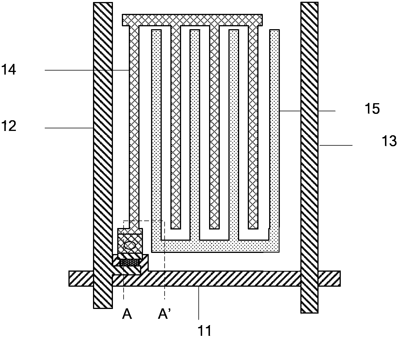
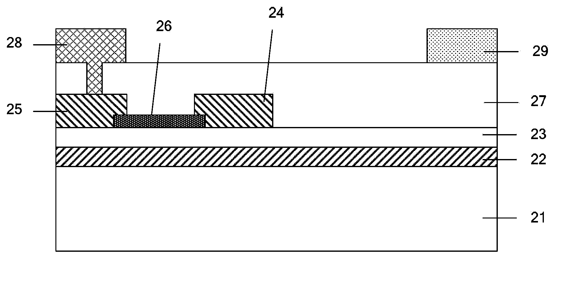
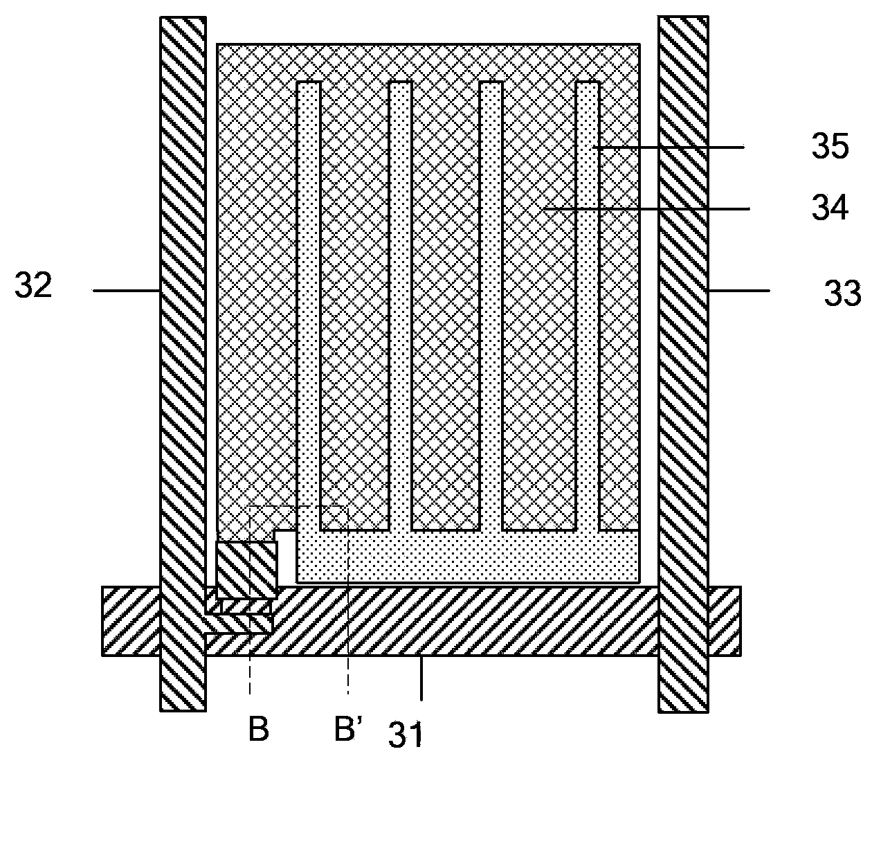
[0051] The basic idea of ​​the present invention is: the pixel structure includes: a first thin film transistor, a second thin film transistor, a gate line, a data line, a common line, a pixel electrode and a common electrode; wherein, the gate of the first thin film transistor is connected to the gate line , the drain is connected to the pixel electrode, the source is connected to the data line; the gate of the second thin film transistor is connected to the gate line, the drain is connected to the common electrode, and the source is connected to the common line.

[0052] Figure 5 It is a schematic diagram of an IPS pixel structure according to an embodiment of the present invention, such as Figure 5 As shown, the pixel structure includes: a first thin film transistor 51, a second thin film transistor 52, a gate line 53, a data line 54, a common line 55, a pixel electrode 56 and a common electrode 57; wherein,

[0053] The gate of the first thin film transistor 51 is conne...


PUM


Abstract

The invention discloses a pixel structure. The pixel structure comprises a first thin film transistor, a second thin film transistor, a grid line, a data line, a common line, a pixel electrode and a common electrode, wherein according to the first thin film transistor, a grid is connected with the grid line, a drain is connected with the pixel electrode, and a source is connected with the data line; according to the second thin film transistor, a grid is connected with the grid line, a drain is connected with the common electrode, and the source is connected with the common line. The invention correspondingly discloses an array substrate, display device and pixel structure manufacturing method. By means of the pixel structure and the array substrate, display device and pixel structure manufacturing method, the pixel electrode and the common electrode can both generate completely the same leaping voltage so as to guarantee stability of leaping voltage on a liquid crystal, so that the influence of leaping voltage caused by coupling capacitance on liquid crystal display is completely eliminated, conditions of image flicker and image display non-uniformity are avoided, and image qualities are improved.

Description

technical field [0001] The present invention relates to the display field, in particular to a pixel structure, an array substrate, a display device and a manufacturing method of the pixel structure. Background technique [0002] Thin Film Transistor Liquid Crystal Display (TFT-LCD) has the characteristics of small size, low power consumption, and no radiation, and occupies a dominant position in the current flat panel display market. TFT-LCD is mainly composed of an array substrate and a color filter substrate in a pair of boxes, in which gate lines (Gate lines), data lines (Data lines), pixel electrodes and thin film transistors are formed on the array substrate, and each pixel electrode is controlled by a thin film transistor. . When the thin film transistor is turned on, the pixel electrode is charged during the on time, and after the thin film transistor is turned off, the voltage of the pixel electrode will be maintained until recharging in the next scan. [0003] At ...

Claims


Application Information

Patent Timeline
Patent Type & Authority Applications(China)
IPC IPC(8): G02F1/1362G02F1/1368H01L27/12H01L21/77
Inventor 薛海林王磊李月曹起薛艳娜
Owner BEIJING BOE OPTOELECTRONCIS TECH CO LTD
Why Eureka
Try Eureka