Filling method for redundancy graph

A technology of redundant graphics and filling methods, applied in special data processing applications, instruments, electrical digital data processing, etc., to achieve the effects of improving line width uniformity, increasing graphic density, and improving flatness

Inactive Publication Date: 2014-06-25
SHANGHAI HUALI MICROELECTRONICS CORP
View PDF7 Cites 11 Cited by
  • Summary
  • Abstract
  • Description
  • Claims
  • Application Information

AI Technical Summary

Problems solved by technology

[0011] This patent is mainly used to adjust the density of chip graphics, but it does not involve filling redundant graphics on the entire layout first, then selecting the forbidden area of ​​redundant graphics, and then using Boolean operations to remove redundant graphics located in the forbidden area. Thereby increasing the pattern density on the layout

Method used


Image

  • Filling method for redundancy graph
  • Filling method for redundancy graph
  • Filling method for redundancy graph

Examples


Embodiment 1

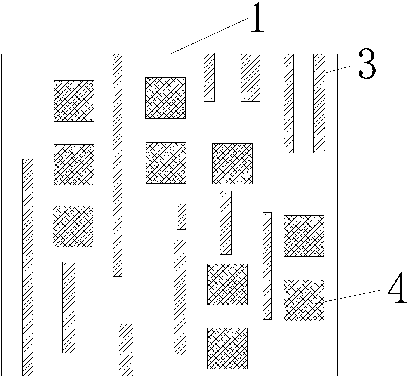
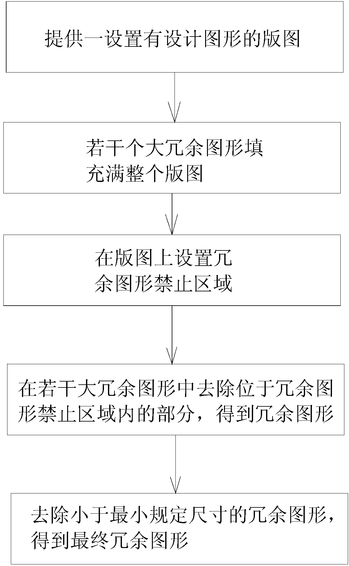
[0040] figure 2 It is the process flow chart of the present invention. The present invention discloses a method for filling redundant graphics, such as figure 2 Shown:

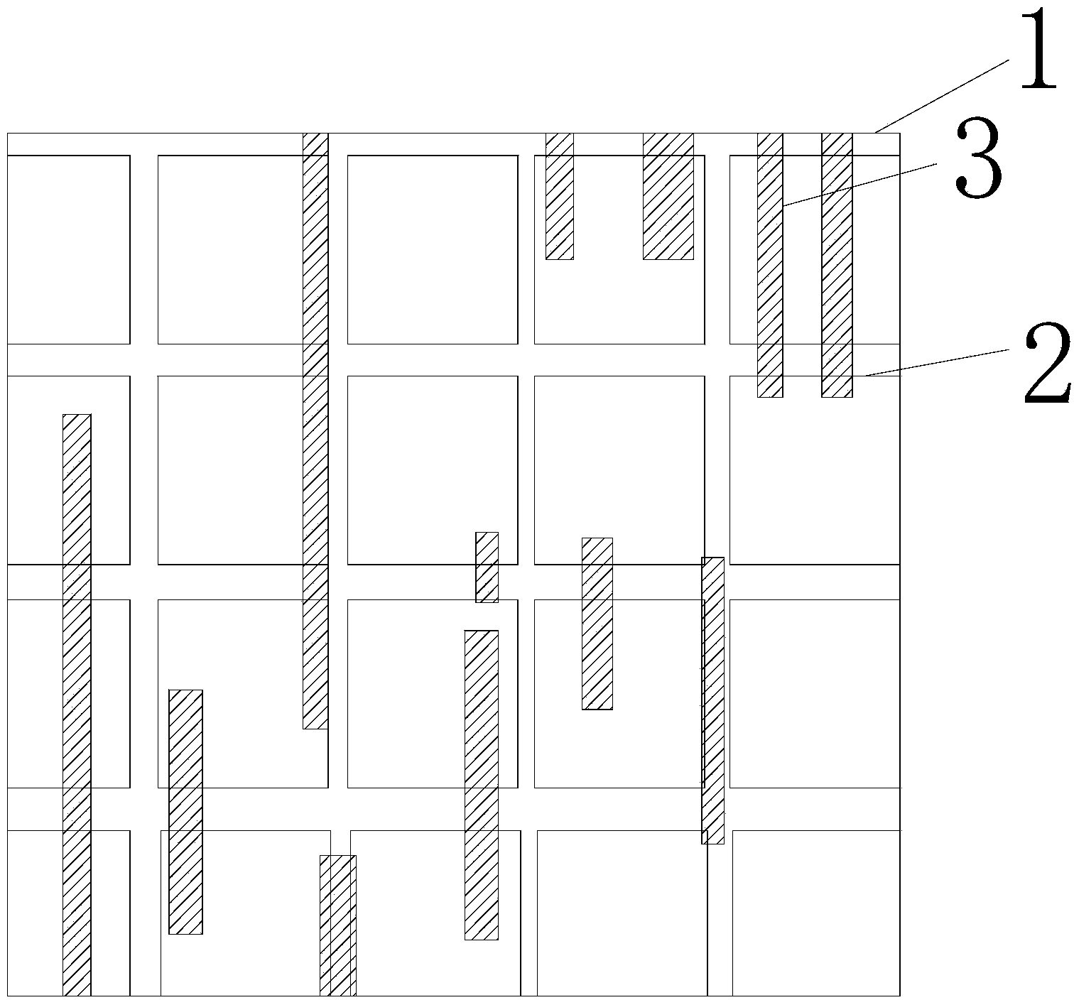
[0041] Step 1: Provide a version with design graphics 3 figure 1 ,Version figure 1 It includes an active layer, a polysilicon layer, a gate layer, and a metal layer. Specifically, an active layer is provided as the lowermost layer of the layout, and the polysilicon layer, the gate layer, and the metal layer are arranged on the active layer from bottom to top. Surface; design graphics 3 are all polygons.

[0042] Step 2: Fill the entire layout with a number of redundant graphics separated by a certain distance from each other. The redundant graphics are polygons. Specifically, the size of the redundant graphics is set by the maximum specified size specified in the layout design rules. Among them, the layout Design rules stipulate various process requirements in layout design (each manufacturer has different layout...


PUM


Abstract

The invention provides a filling method for a redundancy graph. Through software for filling the redundancy graph, firstly, the whole area of a domain is filled with the redundancy graph; secondly, a prohibited area of the redundancy graph is selected; thirdly, the redundancy graph located in the prohibited area is removed through the Boolean operation. By means of the method, filling of the redundancy graph with the larger area can be achieved, the graph density of the whole domain is improved, and therefore line width uniformity of a wafer after the wafer is etched and flatness of the wafer after chemical machinery grinding are improved.

Description

Technical field [0001] The invention relates to the field of semiconductor manufacturing, in particular to a method for filling redundant patterns. Background technique [0002] In the semiconductor layout, the pattern density has a direct impact on the etching and grinding processes; a sufficiently high pattern density helps to improve the uniformity of the pattern density of the layout, thereby ensuring the uniformity of the line width after the photoresist etching and the grinding The flatness of the wafer surface therefore has an important influence on the wafer yield. [0003] With the continuous reduction of semiconductor technology nodes, the pattern density of the layout has an increasing influence on the yield rate. Therefore, semiconductor practitioners need to add redundant patterns around the design pattern to increase the pattern density of the layout, that is, the pattern density of the layout. = (Design graphic area + redundant graphic area) / design rule check area...

Claims


Application Information

Patent Timeline
Patent Type & Authority Applications(China)
IPC IPC(8): G06F17/50
Inventor 陈权于世瑞郜彬
Owner SHANGHAI HUALI MICROELECTRONICS CORP
Why Eureka
Try Eureka