Edge ring of etching device

A technology of etching equipment and edge ring, applied in the field of edge ring, can solve problems such as cavity pollution, weak adhesion, polymer peeling, etc., and achieve the effect of cleaning cycle guarantee, guaranteed yield, and reduced obstruction

Active Publication Date: 2014-06-25
SHANGHAI HUALI MICROELECTRONICS CORP
View PDF7 Cites 2 Cited by
  • Summary
  • Abstract
  • Description
  • Claims
  • Application Information

AI Technical Summary

Problems solved by technology

In addition, the etching residue itself is adhesive, which further strengthens the adhesion of the residue, so that the edge of the upper surface of the edge ring accumulates more and more, and finally the polymer peels off due to weak adhesion. causing contamination of the cavity

Method used


Image

  • Edge ring of etching device
  • Edge ring of etching device
  • Edge ring of etching device

Examples


Embodiment 1

[0026] In this embodiment, an edge ring in the prior art is introduced first.

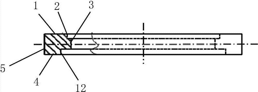
[0027] see figure 1 , figure 1It is a structural cross-sectional view of an edge ring in the prior art, and an example of an edge ring disclosed by a Lam Research Corporation (Lam Research Co., Ltd.) model is a machine of LAM AL-PAD Metal. As shown in the figure, the edge ring is horizontally arranged above the cathode in the cavity of the etching equipment during use, and shields and protects the cathode from plasma bombardment; the edge ring has upper and lower surfaces 1, 4 and vertical etc. High side 5, the edge ring is provided with a central through hole 3 surrounding the substrate, the through hole 3 is located on the upper surface of the edge ring 1, and the orifice is provided with a concentric upper step hole 2 for converging radio frequency energy, and the through hole 3 is located on the lower surface of the edge ring 4 The orifice is provided with a concentric lower stepped hole 12 f...

Embodiment 2

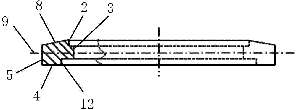
[0034] In this example, see Figure 4 , Figure 4 It is a cross-sectional view of another partial structure of an edge ring of an etching device in the present invention with a slope on its upper surface. As shown in the figure, the upper surface of the edge ring of the present invention has a slope 10 that slopes downward in the direction of the side surface 5 . The starting point of the inclined plane 10 is located at the horizontal center position between the upper stepped hole 2 of the edge ring and the side surface 5, and intersects with the side surface 5 of the edge ring. If the length of the bevel is further shortened, the effect of the bevel will not be brought into full play, and the etching products will also accumulate near the plane position of the upper surface of the edge ring before the start of the bevel structure. In this example, the angle between the inclined plane 10 and the horizontal plane is 45 degrees. A larger inclination angle will weaken the driv...

Embodiment 3

[0036] In this example, see Figure 5 , Figure 5 It is a sectional view of a partial structure of an edge ring of an etching device in the present invention with an arc surface. As shown in the figure, the upper surface of the edge ring of the present invention has a downwardly inclined arc surface 11 towards the side surface 5 . In this example, the arc surface 11 is processed into a parabolic shape. The arc surface 11 starts at the opening of the upper stepped hole 2 of the edge ring and is tangent to the side surface 5. The highest point of the arc surface 11 on the horizontal plane is located at the upper stepped hole 2. at the orifice. The parabola symmetry axis of the parabola of the arc surface 11 is parallel to the horizontal plane, and the parabola apex of the parabola is located at the point of tangency with the side surface 5 . The point of tangency between the arc surface 11 and the side surface 5 should be located above the horizontal centerline 9 of the edge ...


PUM


Abstract

The invention discloses an edge ring of an etching device. According to the edge ring of the etching device, the horizontal plane of the upper surface of an existing edge ring is improved into a plane which is oblique downwards, the flowing direction of airflow passing through the upper surface of the edge ring is changed, the defect that airflow can be blocked by the horizontal plane of the upper surface of the existing edge ring is overcome, products obtained through etching can be easily sucked and taken away by a molecular pump along the plane oblique downwards of the edge ring under the driving of the airflow which can turn along the oblique plane in a cavity, the problem that the products obtained through etching can be accumulated on the upper surface of the existing edge ring and can be stripped from the upper surface of the existing edge ring is solved, the cleaning period of a machine is guaranteed, and the production rate is increased. Meanwhile, the risk of pollution, caused by stripping of polymers, to the cavity is lowered obviously, and it is guaranteed that a high yield is obtained.

Description

technical field [0001] The invention relates to an edge ring of semiconductor etching equipment, more particularly, to an improved structure of an edge ring of semiconductor etching equipment that can eliminate the accumulation and peeling defects of etching products thereon. Background technique [0002] Dry etching is used for fine etching of small feature sizes in advanced circuits in semiconductor manufacturing processes. It refers to the use of reactive gases as the main medium to form plasma under the action of a radio frequency (RF) electric field to etch semiconductor materials. , to obtain the desired device shape structure. Dry etching mainly includes plasma etching, ion milling and reactive ion etching, and many different types of etching equipment have been manufactured. [0003] Generally, in the reaction chamber of various dry etching equipment, the substrate can be fixed on the cathode by mechanical method or electrostatic force. Usually the planar dimension...

Claims


Application Information

Patent Timeline
Patent Type & Authority Applications(China)
IPC IPC(8): H01J37/32H01L21/67
Inventor 江森林阚保国
Owner SHANGHAI HUALI MICROELECTRONICS CORP
Why Eureka
Try Eureka