Method for reducing GaN epitaxial defects through wet etching
A technology of epitaxial defect and wet etching, which is applied in the direction of electrical components, circuits, semiconductor devices, etc., can solve problems such as screw dislocations that cannot be alleviated, achieve good control of corrosion effects, reduce material prices, and improve crystal quality.
- Summary
- Abstract
- Description
- Claims
- Application Information
AI Technical Summary
Problems solved by technology
Method used
Image

Examples
Embodiment Construction
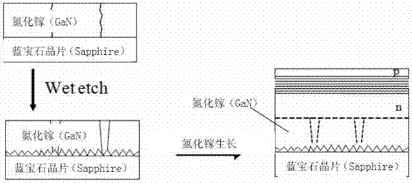
[0031] see figure 1 — Figure 5 , the invention provides a method for reducing GaN epitaxial defects by wet etching, comprising the following steps:
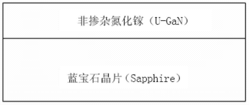
[0032] 1) Growing non-doped gallium nitride on a sapphire wafer; the specific steps are:
[0033] 1.1) Put the sapphire wafer into MOCVD;
[0034] 1.2) Adjust the temperature in MOCVD to 500-600°C and the pressure to 600 Torr, so that GaN can grow 30nm on the sapphire wafer;
[0035] 1.3) Raise the temperature in MOCVD to 1000-1100°C and pressure 400 Torr to grow non-doped gallium nitride 1.2um.
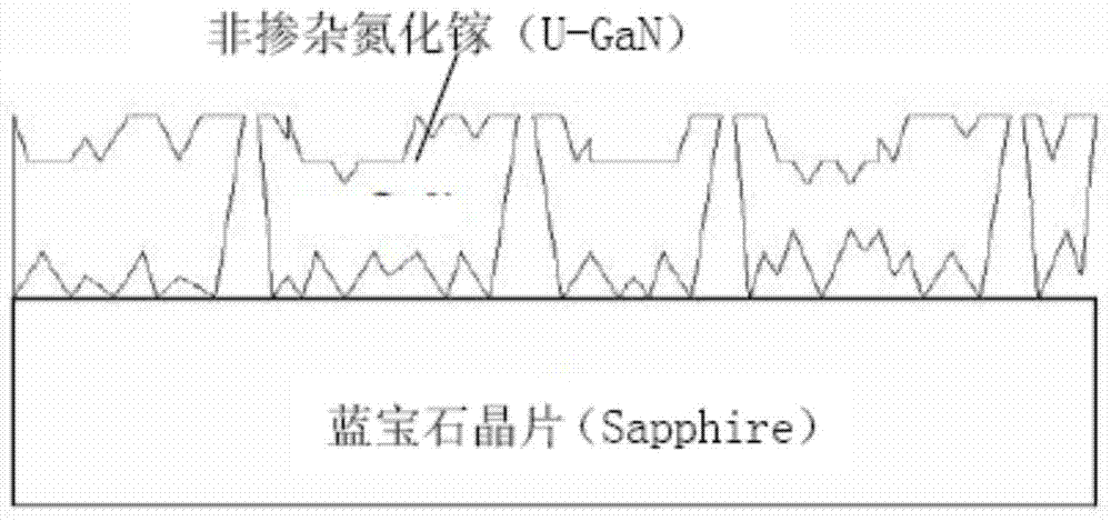
[0036] 2) Put the sapphire wafer into the acidic solution, then take it out and wash it with ionized water and dry it; the time for the sapphire wafer to be placed in the acidic solution is 10-60 minutes, and the temperature of the acidic solution is 100-300°C. Acidic solution is H 3 PO 4 . Sapphire wafer into H 3 PO 4 Solution time is 15 min, H 3 PO 4 The temperature of the solution was 200°C.
[0037] 3) The sapphire wafe...
PUM
 Abstract
Description
Claims
Application Information