An off-line monitoring method for nitrogen-doped silicon carbide thin films

A silicon carbide and nitrogen doping technology, used in electrical components, circuits, semiconductor/solid-state device testing/measurement, etc., can solve the problems such as the inability to solve the monitoring wafer recycling cost and the inability to reduce the reserve of spare bare wafers, etc. To achieve the effect of saving recovery costs

Active Publication Date: 2017-01-04
SHANGHAI HUALI MICROELECTRONICS CORP
View PDF5 Cites 0 Cited by
  • Summary
  • Abstract
  • Description
  • Claims
  • Application Information

AI Technical Summary

Problems solved by technology

[0005] Neither of the above two patents can solve the high recycling costs caused by the monitoring wafer being sent out for recycling once it is used, nor can it reduce the factory’s reserve of spare bare die wafers

Method used


Image

  • An off-line monitoring method for nitrogen-doped silicon carbide thin films
  • An off-line monitoring method for nitrogen-doped silicon carbide thin films
  • An off-line monitoring method for nitrogen-doped silicon carbide thin films

Examples


Embodiment Construction

[0029] The present invention will be further described below in conjunction with the accompanying drawings and specific embodiments. Obviously, the described examples are only some examples of the present invention, not all examples. Based on the examples summarized in the present invention, all examples obtained by persons of ordinary skill in the art without making creative efforts belong to the protection scope of the present invention.

[0030] It should be noted that, in the case of no conflict, the examples in the present invention and the features in the examples can be freely combined with each other.

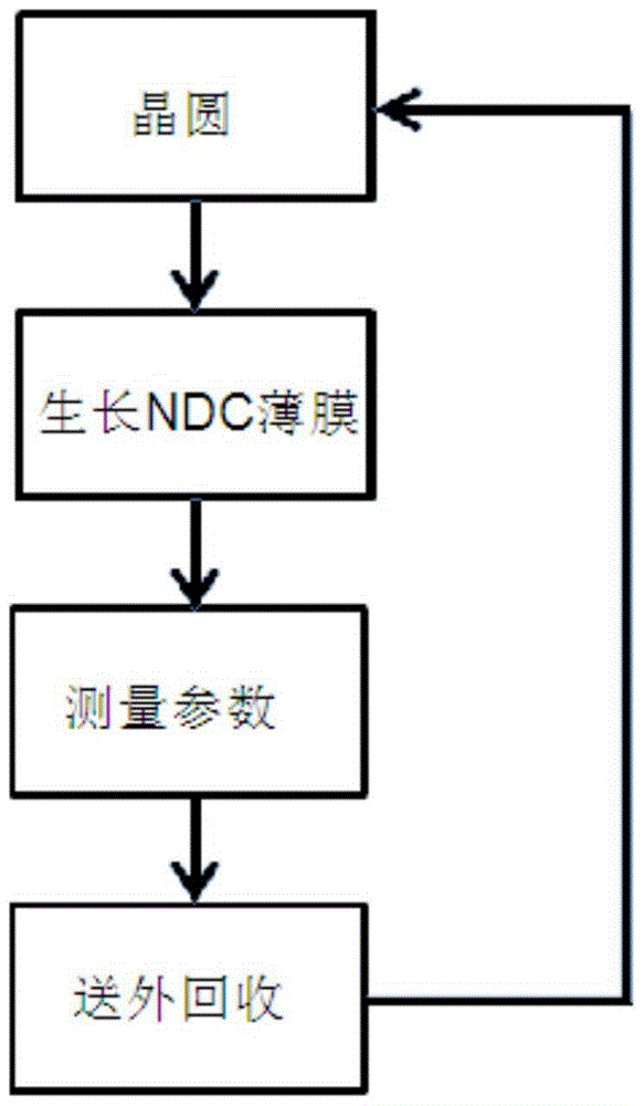
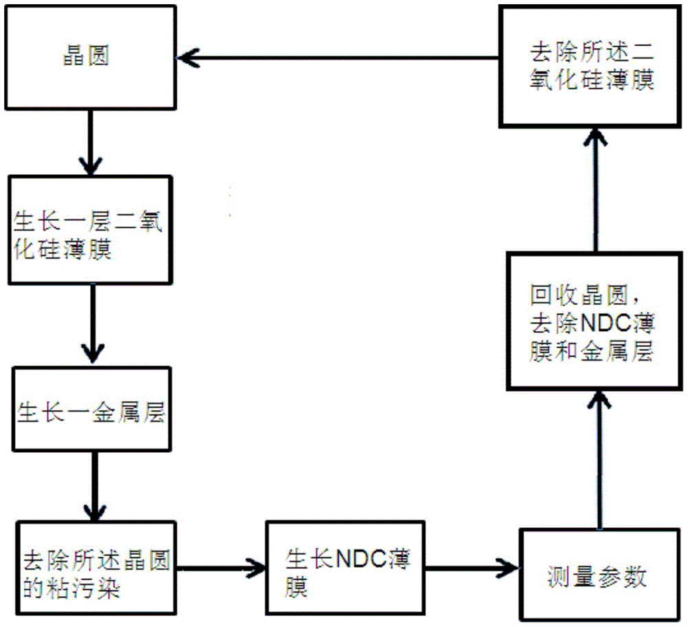
[0031] An example of the invention is an off-line monitoring method for nitrogen-doped silicon carbide films, such as figure 2 shown, including the following steps:

[0032] Step S1, providing a bare wafer;

[0033] Step S2, growing a silicon dioxide film on the bare wafer;

[0034] Step S3, growing a metal layer on the silicon dioxide film;

[0035] Step S4, remov...


PUM


Abstract

The invention provides an off-line monitoring method for a nitrogen-doped silicon carbide film, and relates to the field of semiconductor integrated circuit manufacturing, in particular to the off-line monitoring method for the nitrogen-doped silicon carbide film. The method includes the following steps that a bare wafer is provided; a layer of silicon dioxide film grows on the bare wafer; a metal layer grows on the silicon dioxide film; sticky pollution on the surface of the metal layer is removed; the nitrogen-doped silicon carbide film is manufactured on the metal layer to form a monitoring wafer; parameters are measured; the monitoring wafer is recovered, and the nitrogen-doped silicon carbide film and the metal layer are removed; the silicon dioxide film is removed to form a bare wafer again; the preceding steps are repeated. By means of the method, direct recovery and use of the off-line monitoring wafer of the nitrogen-doped silicon carbide film on a semiconductor production line can be achieved, recovery cost of the off-line monitoring wafer of the nitrogen-doped silicon carbide film is saved, and a large quantity of standby bare wafers do not need to be stored.

Description

technical field [0001] The invention relates to semiconductor integrated circuit manufacturing technology, in particular to an off-line monitoring method for nitrogen-doped silicon carbide film. Background technique [0002] Nitrogen-doped SiC film (N doped SiC, referred to as: NDC) is often used as a dielectric barrier layer at the back end of an integrated circuit to prevent copper from diffusing into the medium. At present, the off-line monitoring of nitrogen-doped silicon carbide film is to directly grow NDC film on the bare wafer, and then use the corresponding optical measuring machine for testing to monitor the thickness, refractive index and other parameters of the film. However, due to the very stable chemical properties of NDC and insoluble in strong acids (it can be dissolved in strong alkali such as NaOH solution, but strong alkali will contaminate silicon wafers), it is impossible to recycle monitoring wafers in the factory using conventional cleaning processes....

Claims


Application Information

Patent Timeline
Patent Type & Authority Patents(China)
IPC IPC(8): H01L21/66
CPCH01L22/30
Inventor 雷通桑宁波
Owner SHANGHAI HUALI MICROELECTRONICS CORP
Why Eureka
Try Eureka