Nano Si/TiO2 ordered array compound photocatalytic water splitting hydrogen preparing cathode material and preparation method thereof
A technology of photo-splitting water to produce hydrogen and ordered arrays, applied in nanotechnology, nanotechnology, nanotechnology for materials and surface science, etc., can solve the problems that hinder the application of crystalline silicon, Si electrodes are easily corroded, and have poor stability and other issues to achieve the effect of improving photocurrent density and chemical stability and improving light absorption performance
- Summary
- Abstract
- Description
- Claims
- Application Information
AI Technical Summary
Problems solved by technology
Method used
Image
Examples
Embodiment 1
[0016] Embodiment 1 A kind of nano-Si / TiO 2 Ordered array composite photo-splitting water hydrogen production cathode material and its preparation method.
[0017] 1. First choose a piece of 2* 2 cm 2 Large and small P-type medium-resistance Si materials are used as the substrate, and the resistivity is 1-10Ω*cm.
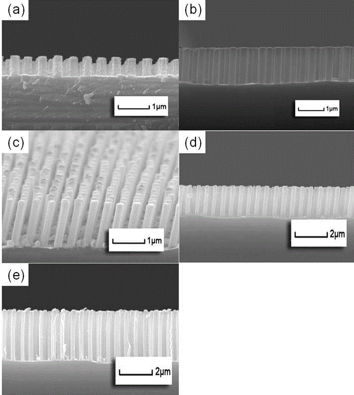
[0018] 2. A two-dimensional hexagonal close-packed structure is formed on the Si substrate by self-assembly of polystyrene spheres with a size of 500 nm on the entire Si substrate. Then reactive ion beam etching was used to etch the polystyrene beads to 280nm-300nm, the etching parameters were flow rate 30Sccm, power 30W, air pressure 74mTorr, and etching time was 280s.
[0019] 3. Deposit 20nm Au as a catalyst on the Si substrate by ion sputtering method, and the deposition current is 10mA.
[0020] 3. Etching the ordered Si nanowire array, the specific process: first mix the HF and H2O2 solutions with a volume ratio of 4:1 evenly, and then put the Si substrate ...
Embodiment 2
[0022] Embodiment 2 A kind of nano-Si / TiO 2 Ordered array composite photo-splitting water hydrogen production cathode material and its preparation method.
[0023] 1. First choose a piece of 2* 2 cm 2 Large and small P-type medium-resistance Si materials are used as the substrate, and the resistivity is 1-10Ω*cm.
[0024] 2. A two-dimensional hexagonal close-packed structure is formed on the Si substrate by self-assembly of polystyrene spheres with a size of 500 nm on the entire Si substrate. Then reactive ion beam etching was used to etch the polystyrene beads to 280nm-300nm, the etching parameters were flow rate 30Sccm, power 30W, air pressure 74mTorr, and etching time was 280s.
[0025] 3. Deposit 20nm Au as a catalyst on the Si substrate by ion sputtering method, and the deposition current is 10mA.
[0026] 3. Etching the ordered Si nanowire array, the specific process: first, HF and H with a volume ratio of 4:1 2 o 2 The solution is mixed evenly, and then the Si subs...
Embodiment 3
[0028] Example 3 A nano-Si / TiO 2 Ordered array composite photo-splitting water hydrogen production cathode material and its preparation method.
[0029] 1. First choose a piece of 2* 2 cm 2 Large and small P-type medium-resistance Si materials are used as the substrate, and the resistivity is 1-10Ω*cm.
[0030] 2. A two-dimensional hexagonal close-packed structure is formed on the Si substrate by self-assembly of polystyrene spheres with a size of 500 nm on the entire Si substrate. Then reactive ion beam etching was used to etch the polystyrene beads to 280nm-300nm, the etching parameters were flow rate 30Sccm, power 30W, air pressure 74mTorr, and etching time was 280s.
[0031] 3. Deposit 20nm Au as a catalyst on the Si substrate by ion sputtering method, and the deposition current is 10mA.
[0032] 3. Etching the ordered Si nanowire array, the specific process: first, HF and H with a volume ratio of 4:1 2 o 2 The solution is mixed evenly, and then the Si substrate is pu...
PUM
 Abstract
Description
Claims
Application Information


