Etching method for improving uniformity of contact hole line width

A contact hole and line width technology, applied in the field of microelectronics, can solve the problem of unstable uniformity of the line width of the wafer contact hole, and achieve the effect of improving product yield

Active Publication Date: 2014-07-09
SHANGHAI HUALI MICROELECTRONICS CORP
View PDF3 Cites 10 Cited by
  • Summary
  • Abstract
  • Description
  • Claims
  • Application Information

AI Technical Summary

Problems solved by technology

However, prior art solutions are in actual mass production, such as figure 1 Shown, the homogeneity of the contact

Method used


Image

  • Etching method for improving uniformity of contact hole line width
  • Etching method for improving uniformity of contact hole line width
  • Etching method for improving uniformity of contact hole line width

Examples


Embodiment Construction

[0041] In order to make the above objects, features and advantages of the present invention more comprehensible, specific implementations of the present invention will be described in detail below in conjunction with the accompanying drawings.

[0042] In the following description, numerous specific details are set forth in order to provide a thorough understanding of the present invention. However, the present invention can be implemented in many other ways different from those described here, and those skilled in the art can make similar extensions without violating the connotation of the present invention, so the present invention is not limited by the specific implementations disclosed below.

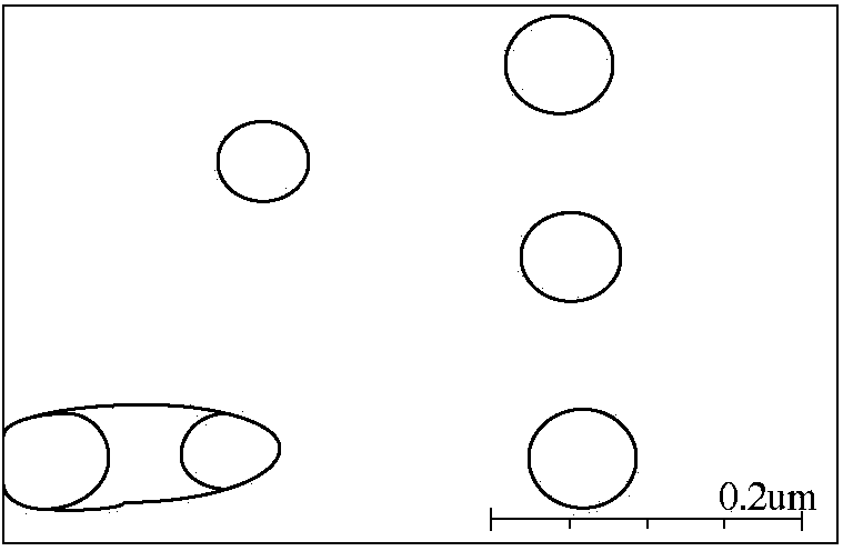
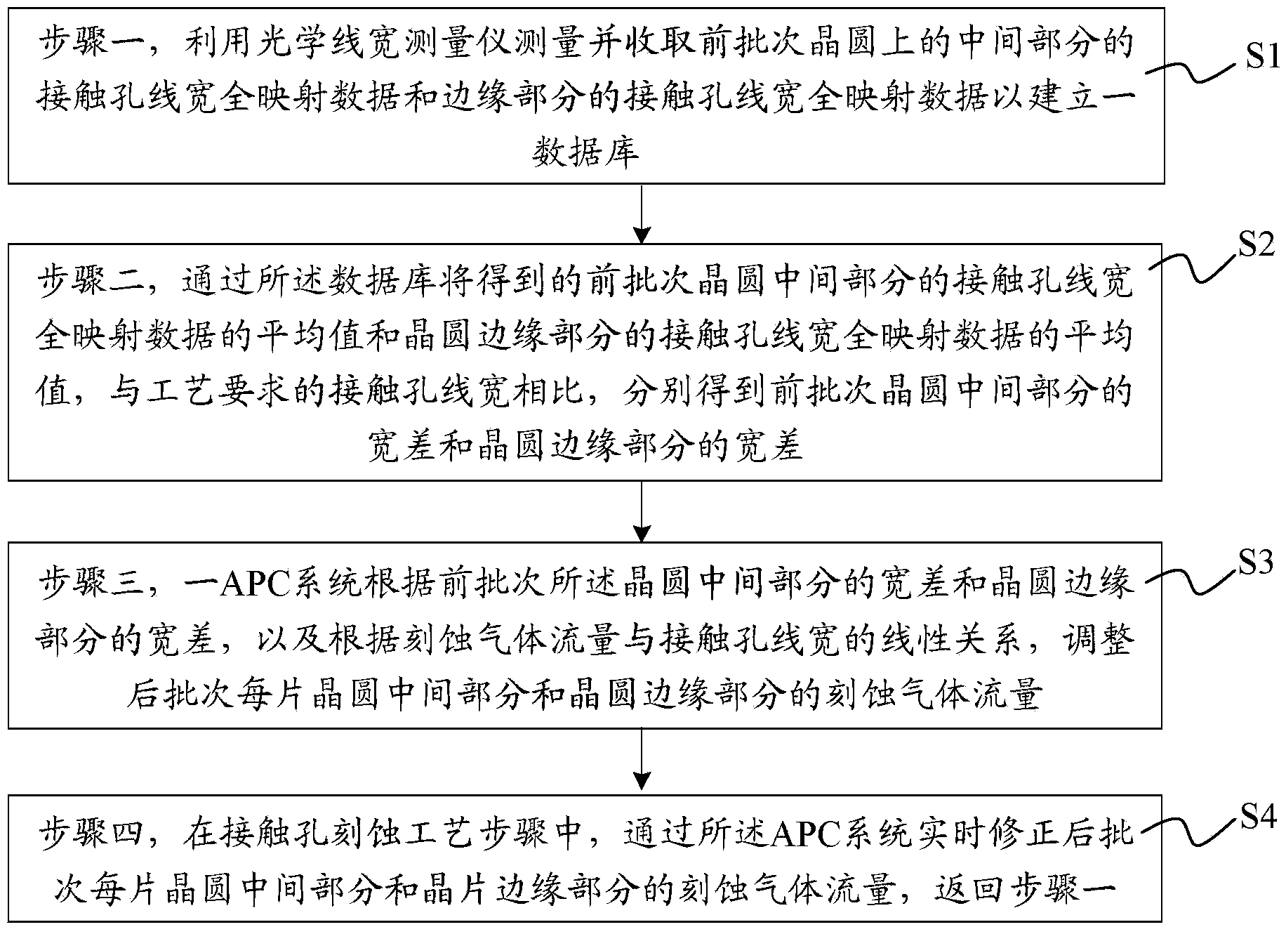
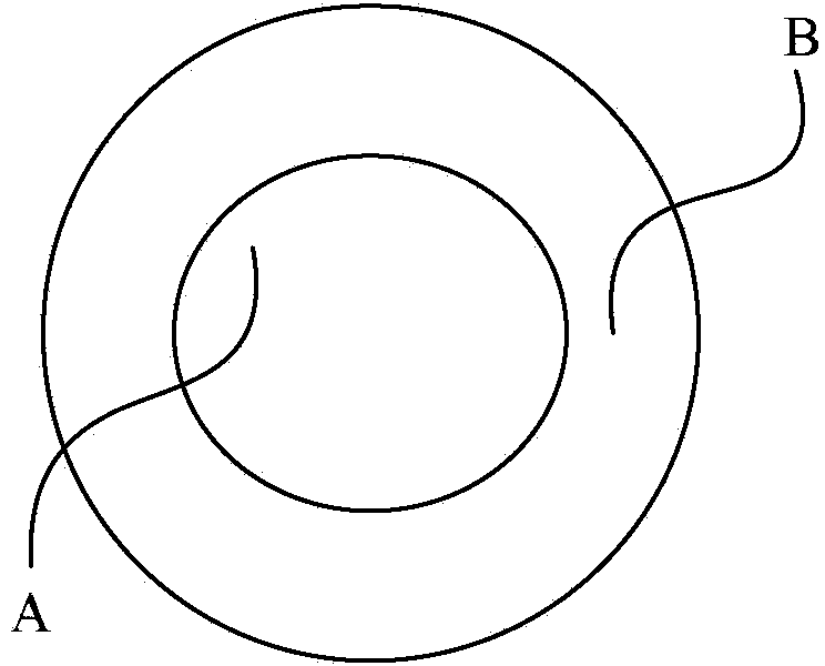
[0043] Specifically, figure 2 A flow chart of an etching method for improving line width uniformity of a contact hole according to an embodiment of the present invention is schematically shown.

[0044] Such as figure 2 shown, combined with Figure 3-6 , the etching method for ...


PUM


Abstract

The invention provides an etching method for improving the uniformity of the contact hole line width. The method comprises the steps that an optical line width measurement instrument is used for measuring and collecting contact hole line width full-mapping data on wafers of the prior batch, so that a database is established; the average value of the contact hole line width full-mapping data of the middle portions of the wafers of the prior batch and the contact hole line width full-mapping data of the edges of the wafers of the prior batch is compared with the value of the contact hole line width required by the technology through the database, so that the width difference of the middle portions of the wafers of the prior batch and the width difference of the edges of the wafers of the prior batch are obtained respectively; according to the width difference of the middle portions of the wafers of the prior batch and the width difference of the edges of the wafers of the prior batch, the etching gas flow of the middle portions of wafers of a later batch and the etching gas flow of the edges of the wafers of the later batch are respectively adjusted through an APC system; in the contact hole etching technology steps, the etching gas flow of the wafers of the later batch is corrected in real time through the APC system, so that influence, caused by the photoetching difference of the wafers of the prior batch, on photoetching of the wafers of the later batch can be avoided, the shortages that the gas flow of the middle portions and the edges of the wafers is not changed in the contact hole etching technology are overcome, and the gas flow change of each portion is accurately mastered.

Description

technical field [0001] The invention belongs to the technical field of microelectronics, in particular to an etching method for improving the line width uniformity of a contact hole. Background technique [0002] In the 12-inch 65nm and below process technology, the formation of contact holes is always a challenging process, and the conduction of contact holes directly affects the realization of chip functions. However, the process technology of lithography registration accuracy has faced a bottleneck, and there is little room for improvement. With the continuous update of the technology nodes forming the wafer, not only the contact holes are getting smaller and denser, but the size of the wafer is also increasing. These factors will cause risks to the conduction of the contact holes. [0003] At present, the current technical solution for forming contact holes is as follows: During the development of contact hole etching programs, use a common line width measuring instrume...

Claims


Application Information

Patent Timeline
IPC IPC(8): H01L21/768H01L21/66
CPCH01L21/76816H01L22/26H01L2221/101
Inventor 高腾飞荆泉张颂周任昱吕煜坤张旭升
Owner SHANGHAI HUALI MICROELECTRONICS CORP
Why Eureka
Try Eureka