Nitride semiconductor light emitting device and method of manufacturing the same

A technology for nitride semiconductors and light-emitting devices, applied in semiconductor devices, electrical components, circuits, etc., can solve problems such as poor adhesion and decreased bonding reliability, and achieve improved adhesion characteristics, long-term reliability, and improved optical properties. Effects of Scattering Properties

Inactive Publication Date: 2014-07-09
ILJIN LED
View PDF1 Cites 4 Cited by
  • Summary
  • Abstract
  • Description
  • Claims
  • Application Information

AI Technical Summary

Problems solved by technology

[0004] However, in the nitride semiconductor light emitting device having the above-mentioned structure, the transparent conductive pattern is formed on the current disconnection pattern composed of an insulating substance. In this case, since the transparent conductive pattern and the p-electrode pad are respectively made of metal series Composition, so there is a problem that the joint reliability drops sharply due to the poor adhesion between each other

Method used


Image

  • Nitride semiconductor light emitting device and method of manufacturing the same
  • Nitride semiconductor light emitting device and method of manufacturing the same
  • Nitride semiconductor light emitting device and method of manufacturing the same

Examples


Embodiment Construction

[0027] Hereinafter, referring to the accompanying drawings, a nitride semiconductor light emitting device and a manufacturing method thereof according to preferred embodiments of the present invention will be described in detail as follows.

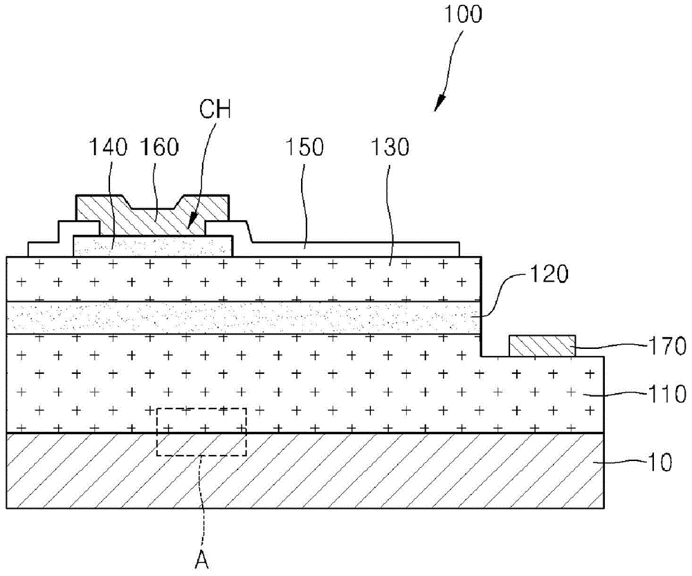
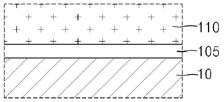
[0028] figure 1 is a sectional view showing a nitride semiconductor light emitting device according to an embodiment of the present invention, figure 2 for figure 1 A magnified view of part A of .

[0029] refer to figure 1 and figure 2 , the nitride semiconductor light emitting device 100 shown in the embodiment of the present invention includes: n-type nitride layer 110, active layer 120, p-type nitride layer 130, current disconnection pattern 140, transparent conductive pattern 150, p-electrode plate 160 and n-electrode plate 170 . Also, the nitride semiconductor light emitting device 100 of the embodiment of the present invention may further include a buffer layer 105 .

[0030] The n-type nitride layer 110 is formed on the su...


PUM

PropertyMeasurementUnit
thicknessaaaaaaaaaa

Abstract

The present invention provides a nitride semiconductor light emitting device which can improve long term durability by securing excellent light scattering capabilities while enhancing adhesion of a p-electrode pad and a current blocking pattern, and a method of manufacturing the same. The nitride semiconductor light emitting device includes an n-type nitride layer; an active layer formed on the n-type nitride layer; a p-type nitride layer formed on the active layer; a current blocking pattern formed on the p-type nitride layer; a transparent conductive pattern formed to cover upper sides of the p-type nitride layer and the current blocking pattern, and having a contact hole through which a portion of the current blocking pattern is exposed; and a p-electrode pad formed on the current blocking pattern and the transparent conductive pattern, and directly connected to the current blocking pattern.

Description

technical field [0001] The present invention relates to a nitride semiconductor light-emitting device and a manufacturing method thereof, and more specifically, to a nitride semiconductor light-emitting device having excellent light scattering properties and bonding properties and a manufacturing method thereof. Background technique [0002] Recently, gallium nitride (GaN)-based nitride semiconductor light-emitting devices have been mainly studied as nitride semiconductor light-emitting devices. This GaN-based nitride semiconductor light-emitting device is used in blue and green light-emitting diode (LED) light-emitting devices, metal-semiconductor field-effect transistors (MESFET, Metal-Semiconductor FET), high electron mobility transistors ( HEMT, High Electron Mobility Transistor) and other high-speed switches and high-power devices. [0003] In order to improve the light efficiency of the nitride semiconductor light emitting device, a transparent conductive pattern is f...

Claims


Application Information

Patent Timeline
Patent Type & Authority Applications(China)
IPC IPC(8): H01L33/38H01L33/14H01L33/00
CPCH01L33/145H01L33/38H01L33/42H01L33/36
Inventor 金升龙洪政佑
Owner ILJIN LED
Why Eureka
Try Eureka