Printed wiring board and method of producing the same

A circuit board and conductor circuit technology, which is applied in the fields of printed circuit manufacturing, printed circuit, multi-layer circuit manufacturing, etc., can solve the problem of poor bonding performance between conductor circuit and solder barrier layer, smaller contact area, conductor circuit and solder barrier In order to reduce resin residues, improve metal bonding characteristics, and prevent the reduction of bonding strength

Inactive Publication Date: 2008-01-16
IBIDEN CO LTD
View PDF0 Cites 4 Cited by
  • Summary
  • Abstract
  • Description
  • Claims
  • Application Information

AI Technical Summary

Problems solved by technology

[0014] However, in finely wired conductor circuits, the contact area between the conductor circuit and the solder barrier layer becomes significantly smaller, and therefore, the adhesive performance between the conductor circuit and the solder barrier layer deteriorates
In particular, when the conductor circuit is formed on the surface layer of the printed circuit board in a rough state, the adhesion between the conductor circuit and the solder barrier layer is worse

Method used


Image

  • Printed wiring board and method of producing the same
  • Printed wiring board and method of producing the same
  • Printed wiring board and method of producing the same

Examples


example 1

[0193]Preparation of adhesive layer for electroless plating

[0194] (1) 35 parts by weight of the acrylated product of 25wt% cresol novolak type epoxy resin with a molecular weight of 2500 manufactured by Nippon Kayaku Corporation and 3.15 parts by weight of Aronics M315 manufactured by Toa Gosei Corporation The photosensitive monomer, 0.5 parts by weight of S-65 defoamer manufactured by Sannopuco and 3.6 parts by weight of N-methylpyrrolidone (NMP) were mixed with stirring.

[0195] (2) 12 parts by weight of polyethersulfone (PES) and 7.2 parts by weight of the epoxy resin particles manufactured by Sanyo Kasei under the trade name Polymerpol with an average particle size of 0.1 μm and 3.09 parts by weight whose average particle size is 0.5μm of the same epoxy resin, particles are mixed and 30 parts by weight of NMP are added and mixed with a ball mill under stirring.

[0196] (3) 2 parts by weight of an imidazole curing agent manufactured by Shikoku Kasei under the trade name 2...

example 2

[0244] According to the steps (1) and (2) in Example 1, the core board 31 with the roughened surface of the conductor circuit shown in FIG. 21 was prepared. On the other hand, the single-sided circuit board 15 shown in FIGS. 13-17 is prepared.

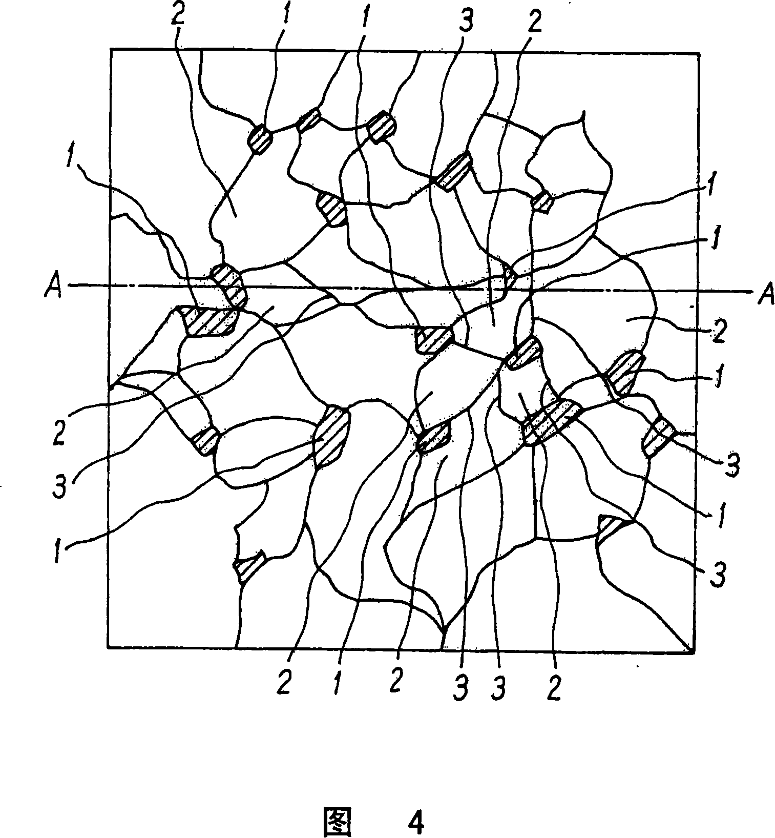
[0245] The specific preparation of the single-sided circuit board 15 is as follows. 12μm thick copper foil 6 is placed on the glass epoxy substrate 5 to form a single-sided copper-clad board 7, as shown in Figure 13. The surface of the copper-clad board 7 not covered with copper foil 6 is exposed to CO 2 Under the gas laser beam, an opening 8 with a diameter of 50 μm is formed, as shown in FIG. 14.

[0246] After that, under the conditions listed in step (11) of Example 1, the copper-clad plate 7 was electroplated to form a plating film 9 as shown in FIG. 15. After that, a stainless printing mask with an opening of 1.0 μm in diameter corresponding to the position of the through hole is placed, and Au-Pd conductive paste manufactured by Tan...

example 3

[0250] Repeat the manufacturing process steps of Example 1, except that the roughened surface of the lower conductor circuit is not replaced with tin, and the metal layer is made of other non-oxidizing metals, or no metal layer is formed. The heating test and thermal cycle test were performed on the finished circuit board in the same manner as in Example 1. The results are listed in Table 2.


PUM


Abstract

A multilayer printed wiring board (52) provided with a lower layer conductor circuit (26), an interlayer resin insulating layer (37) formed on the lower layer conductor circuit (26), an upper layer conductor circuit (44) formed on the interlayer resin insulating layer (37) and via-holes (51) connecting the lower layer conductor circuit (26) to the upper layer conductor circuit (44), wherein the lower layer conductor circuit (26) has a roughed surface (35) formed with an etchant containing a cupric complex and an organic acid, and the via-holes (51) are connected to the lower layer conductor circuit (26) through the roughed surface (35). Tight adhesion between the lower layer conductor circuit and the interlayer resin insulating layer and between the lower layer conductor circuit and the via-hole conductors can be improved and the high connection reliability of the via-hole parts is ensured even during heating or through heat cycle.

Description

[0001] This application is a divisional application for an invention patent application with an application date of July 8, 1998, an application number of 98806974.1, and an invention title of "Printed Circuit Board and Its Manufacturing Method". Technical field [0002] The present invention relates to a printed circuit board, in particular to a multilayer printed circuit board. Even under heating or thermal cycling, it can prevent the interlayer resin insulation layer from peeling off and ensure the connection reliability of the through-hole portion. Furthermore, the present invention relates to a printed circuit board having excellent adhesion performance between the pad conductor circuit and the solder barrier layer. Background technique [0003] Recently, with the demand for high density of multilayer circuit boards, so-called stacked multilayer circuit boards have attracted attention. A stacked multi-layer circuit board has been manufactured by the method disclosed in JP-B-4...

Claims


Application Information

Patent Timeline
Patent Type & Authority Applications(China)
IPC IPC(8): H05K3/46H05K3/38H05K1/11H05K3/00H05K3/28H05K3/42
CPCH05K2203/121H05K2203/072H05K3/421H05K1/112Y10S428/901H05K3/4614H05K3/384H05K3/4661H05K3/28H05K3/383H05K2203/0307H05K3/0094Y10T428/24917H05K3/46
Inventor 三门幸信平松靖二袁本镇
Owner IBIDEN CO LTD
Why Eureka
Try Eureka