Polycrystalline silicon and preparation method thereof

A technology of polysilicon and polysilicon wafers, which is applied in the field of polysilicon and its preparation, can solve the problems of not being able to obtain high-quality complete polysilicon materials, and achieve the effects of less crystal growth dislocation, improved utilization rate, and appropriate grain boundaries

Inactive Publication Date: 2014-07-16
NANTONG ZONGYI NEW MATERIAL
View PDF7 Cites 4 Cited by
  • Summary
  • Abstract
  • Description
  • Claims
  • Application Information

AI Technical Summary

Problems solved by technology

In the production of polysilicon, a large amount of silicon material is put into the crucible furnace to grow crystals. However, in terms of the current production process of polysilicon, it is impossible to obtain high-quality complete polysilicon materials in the ingot production process. The ingot is surrounded by irregular polycrystalline, and there is a blending zone between the single crystal and polycrystalline; or the core is similar to single crystal, and the silicon ingot is surrounded by polycrystalline

Method used


Image

  • Polycrystalline silicon and preparation method thereof
  • Polycrystalline silicon and preparation method thereof
  • Polycrystalline silicon and preparation method thereof

Examples


Embodiment 1

[0026] The method that polysilicon of the present invention prepares adopts, comprises the following steps:

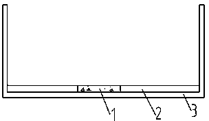
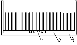
[0027] 1) A number of polysilicon seed crystals are laid in the center of the bottom of the crucible 3 to form a seed layer 1 , the number of polycrystalline seed crystals are closely arranged with each other, and the gap between the several polycrystalline seed crystals is less than 2 mm. Between the seed crystal layer at the bottom of the crucible 3 and the four sides of the crucible, a number of polycrystalline silicon sheets are arranged side by side to form a flat layer 2, and the polycrystalline silicon sheets are scraps of prefabricated polycrystalline silicon ingots. Wherein, the seed crystal layer 1 is arranged in the center of the bottom of the crucible in a square shape, and the cross section of the bottom of the crucible is square; the flat layer 2 adopts a square polysilicon wafer of the same size. When laying, ensure that the seed layer 1 and the paving l...

Embodiment 2

[0031] The method that polysilicon of the present invention prepares adopts, comprises the following steps:

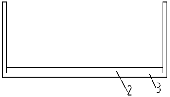
[0032] 1) On the bottom of the crucible 3, a number of polycrystalline silicon wafers are arranged side by side to form a flat layer 2, and the polycrystalline silicon wafers are scraps of prefabricated polycrystalline silicon ingots. Wherein, the tiled layer 2 adopts rectangular polysilicon wafers of the same size and specification, and the thickness of the tiled layer is between 20 mm and 50 mm.

[0033] 2) The silicon material in a molten state is arranged on the flat layer 2 to ensure that the heating temperature at the bottom of the crucible 3 is lower than the melting point of the polysilicon wafer, so that the thickness of the flat layer after the silicon material is melted is equal to that of the pre-laid flat layer 2 1 / 4~1 / 2 of the thickness; among them, the silicon material is solid silicon material, and the temperature in the upper part of the crucible is gu...


PUM

PropertyMeasurementUnit
thicknessaaaaaaaaaa

Abstract

The invention discloses polycrystalline silicon and a preparation method thereof. The preparation method is characterized by comprising the following steps: paving a plurality of polycrystalline silicon seed crystals in the center of the bottom of a crucible to form a seed crystal layer; paving a plurality of parallelly arranged polycrystalline silicon slices between the seed crystal layer positioned at the bottom of the crucible and the periphery of the crucible to form a flat paving layer; arranging silicon materials which are in a molten state on the seed crystal layer and the flat paving layer to ensure that the heating temperature of the bottom of the crucible is lower than the melting points of the polycrystal seed crystals and the polycrystalline silicon slices; and controlling the temperature inside the crucible to gradually form a temperature gradient upwards along the direction of a plane, where the bottom of the crucible is located, to enable molten silicon materials to form crystals on the seed crystal layer and the flat paving layer so as to obtain a polycrystalline silicon ingot with the polycrystalline silicon as a component. By adopting the mode, the preparation method disclosed by the invention has the advantages that long crystals are less misplaced, the crystal boundary is proper, the conversion efficiency of a battery made from the crystal is improved by 0.4-0.9, a prepared silicon ingot is complete polycrystalline silicon, the subsequent stripping of different components is omitted and the utilization ratio of the silicon materials is increased.

Description

technical field [0001] The invention relates to a polysilicon and a preparation method thereof, in particular to a polysilicon obtained from a silicon ingot which is completely polysilicon and a preparation method thereof, belonging to the field of semiconductor preparation. Background technique [0002] Crystalline silicon is a semiconductor material commonly used in the manufacture of solar cells, and the preparation of crystalline silicon is mainly monocrystalline silicon produced by the current Czochralski method and polycrystalline silicon produced by ingot casting technology. Due to the high conversion efficiency of monocrystalline silicon, there are Due to the problem of long production cycle, polysilicon with high cost performance has great market potential in recent years. In the production of polysilicon, a large amount of silicon material is put into the crucible furnace to grow crystals. However, in terms of the current production process of polysilicon, it is im...

Claims


Application Information

Patent Timeline
Patent Type & Authority Applications(China)
IPC IPC(8): C30B28/06C30B29/06
Inventor 李俊军章勇黄涛明
Owner NANTONG ZONGYI NEW MATERIAL
Why Eureka
Try Eureka