Preparation method of punch-through silicon carbide insulated gate bipolar transistor

A technology of bipolar transistor and general-type silicon carbide, which is applied in the field of microelectronics, can solve the problems of high production cost, high energy consumption in the epitaxial process, and high process requirements, so as to save resources and energy, reduce the difficulty of preparation, and save the cost of preparation effect with time

Active Publication Date: 2016-08-17
XIDIAN UNIV
View PDF3 Cites 0 Cited by
  • Summary
  • Abstract
  • Description
  • Claims
  • Application Information

AI Technical Summary

Problems solved by technology

[0007] 1. High preparation cost
For example, SiC epitaxial equipment is expensive, and the epitaxial process consumes a lot of energy, etc.
[0008] 2. The technical difficulty of growing a thicker SiC epitaxial layer is high. For example, for the growth of an epitaxial layer with a thickness of 100 μm and above, the process requirements are high. Only top silicon carbide device companies such as Cree can do it in the world. Therefore, the technology The bottleneck problem limits the popularization and application of high-power SiC IGBT

Method used


Image

  • Preparation method of punch-through silicon carbide insulated gate bipolar transistor
  • Preparation method of punch-through silicon carbide insulated gate bipolar transistor

Examples


Embodiment 1

[0030] Example 1: The dislocation density at the base plane is 10 4 / cm 2 , the substrate concentration is 2×10 14 cm -3 A punch-through silicon carbide insulated gate bipolar transistor was fabricated on a P-type SiC substrate without a micropipe structure.

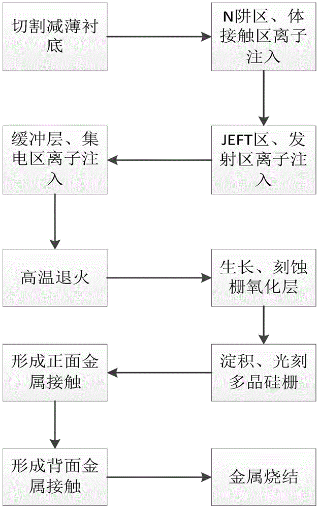
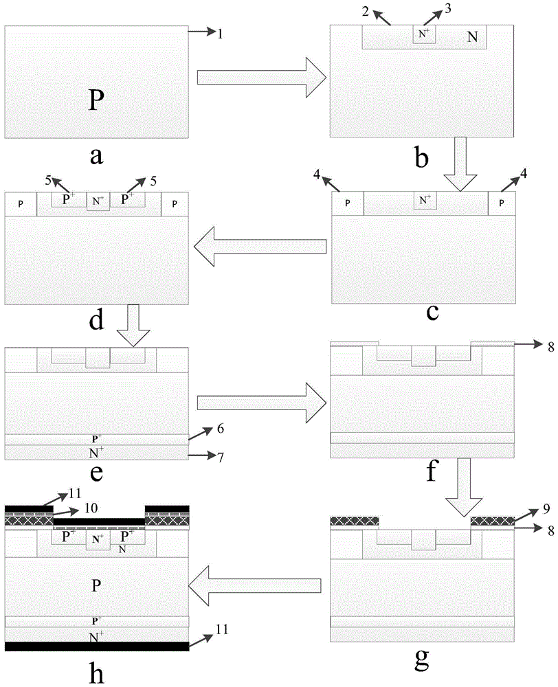
[0031] refer to figure 1 and figure 2 , the implementation steps of this embodiment are as follows:

[0032] Step 1: Substrate processing.

[0033] Cutting and thinning to 100 μm along the back side of the P-type SiC substrate 1, such as figure 2 a; Polish the cutting surface, then wet oxygen oxidation at 950°C for 20 minutes, then remove the oxide layer, and restore the structure and flatness of the cutting surface.

[0034] Step 2: N well ion implantation.

[0035] (2.1) Deposit a layer of SiO with a thickness of 0.2 μm on the front of the P-type SiC substrate by low-pressure chemical vapor deposition 2 , and then deposit Al with a thickness of 1 μm as a barrier layer for nitrogen ion implantation, and apply...

Embodiment 2

[0059] Example 2: The dislocation density at the base plane is 10 4 / cm 2 , the substrate concentration is 6×10 14 cm -3 A punch-through silicon carbide insulated gate bipolar transistor was fabricated on a P-type SiC substrate without a micropipe structure.

[0060] refer to figure 1 and figure 2 , the implementation steps of this embodiment are as follows:

[0061] Step A: Same as Step 1 of Example 1.

[0062] Step B: N-well implantation.

[0063] (b1) is identical with the step (2.1) of embodiment 1;

[0064] (b2) Perform two ion implantations on the front side of the P-type SiC substrate at 650°C, that is, first use 450Kev implantation energy, 5×10 12 cm -2 Implantation dose of nitrogen ion implantation, and then use the implantation energy of 250Kev, 1 × 10 12 cm -2 Implantation dose of the second nitrogen ion implantation, forming N well 2, such as figure 2 b.

[0065] Step C: Apply glue on the front side of the P-type SiC substrate that has completed the ...

Embodiment 3

[0079] Example 3: The dislocation density at the base plane is 10 4 / cm 2 , the substrate concentration is 1×10 15 cm -3 A punch-through silicon carbide insulated gate bipolar transistor was fabricated on a P-type SiC substrate without a micropipe structure.

[0080] refer to figure 1 and figure 2 , the implementation steps of this embodiment are as follows:

[0081] The first step: same as step 1 of embodiment 1.

[0082] Step 2: Deposit a layer of SiO with a thickness of 0.2 μm on the front side of the P-type SiC substrate by low-pressure chemical vapor deposition 2 , and then deposit Al with a thickness of 1 μm as a barrier layer for nitrogen ion implantation, and apply glue to photoetch the window of the N well implantation region; perform two ion implantations on the front side of the P-type SiC substrate at 650 ° C, that is, first use 600Kev Inject energy, 8×10 12 cm -2 Implantation dose of nitrogen ion implantation, and then using the implantation energy of 35...


PUM

PropertyMeasurementUnit
thicknessaaaaaaaaaa
thicknessaaaaaaaaaa
thicknessaaaaaaaaaa

Abstract

The invention discloses a method for preparing a punch-through type silicon carbide insulated gate bipolar transistor. The method mainly solves the problem that at present, the preparing cost of the silicon carbide insulated gate bipolar transistor is too high. The method comprises the implementing steps that (1) a P-type silicon carbide substrate with good structural performance is selected, the back surface of the substrate is cut and thinned, and a cut surface is polished and oxidized; (2) an N well region, an N+ body contact region, a JFET region and a P+ emitter region are formed on the front surface of the substrate in sequence through ion implantation; (3) ion implantation is carried out on a buffer layer and a collector electrode region on the back surface of the substrate; (4) high temperature annealing is carried out, activation is carried out, and dopants are implanted; (5) a grid oxidation layer is grown and etched on the front surface of the substrate, and a polysilicon gate is deposited on the front surface of the substrate; (6) metal deposition and photoetching are carried out on the front surface and the back surface of the substrate, and electrodes are led out. Compared with an existing method, the epitaxial growth of an over-thick withstand voltage layer is not needed, a large amount of production cost is saved, processing steps are simplified, and the method can be applied to the fields of inverters, switch power supplies and illumination circuits.

Description

technical field [0001] The invention belongs to the field of microelectronic technology, and relates to a method for preparing a semiconductor device, in particular to a punch-through SiC IGBT using a substrate as a voltage-resistant layer, which can be widely used in frequency converters, inverters, switching power supplies, lighting circuits and motors and other fields. technical background [0002] Silicon carbide insulated gate bipolar transistor, or SiC IGBT, is a new type of high-voltage resistant device developed based on silicon carbide materials. At present, the mainstream solid-state device used in the field of power electronics is Si IGBT, and its turn-off voltage is 0.6-6.5kV. After 30 years of development, Si IGBT has reached the limit of performance and device structure. With the development of new applications such as electric vehicles, photovoltaic and wind energy green energy, and smart grids, a new leap in the performance of power electronic devices is req...

Claims


Application Information

Patent Timeline
Patent Type & Authority Patents(China)
IPC IPC(8): H01L21/331H01L21/265
CPCH01L29/66068
Inventor 郭辉翟华星宋庆文张艺蒙张玉明汤晓燕
Owner XIDIAN UNIV
Why Eureka
Try Eureka