Method for manufacturing N-channel silicon carbide insulated gate bipolar transistor

A bipolar transistor and silicon carbide technology, applied in the field of microelectronics, can solve the problems of high manufacturing cost, high energy consumption in the epitaxy process, and large on-resistance, so as to save resources and energy, reduce the difficulty of preparation, and save the cost of preparation effect with time

Active Publication Date: 2014-07-16
XIDIAN UNIV
View PDF4 Cites 6 Cited by
  • Summary
  • Abstract
  • Description
  • Claims
  • Application Information

AI Technical Summary

Problems solved by technology

[0005] 1. The P-type substrate acting as the collector has many defects and large on-resistance
[0006] 2. High preparation cost
For example, SiC epitaxial equipment is expensive, and the epitaxial process consumes a lot of energy, etc.
[0007] 3. It is technically difficult to grow thicker epitaxial layers
For the growth of epitaxial layers with a thickness of 100 μm and above, the process requirements are high, which can only be achieved by top silicon carbide device companies such as Cree in the world. Therefore, the technical bottleneck problem limits the popularization and application of high-power N-channel SiC IGBT. application

Method used


Image

  • Method for manufacturing N-channel silicon carbide insulated gate bipolar transistor
  • Method for manufacturing N-channel silicon carbide insulated gate bipolar transistor
  • Method for manufacturing N-channel silicon carbide insulated gate bipolar transistor

Examples


Embodiment 1

[0030] Example 1: Dislocations in the base plane are 10 4 / cm -3 , the substrate concentration is 2×10 14 cm -3 N-channel silicon carbide insulated gate bipolar transistors were prepared on the micropipe-free N-type SiC substrate.

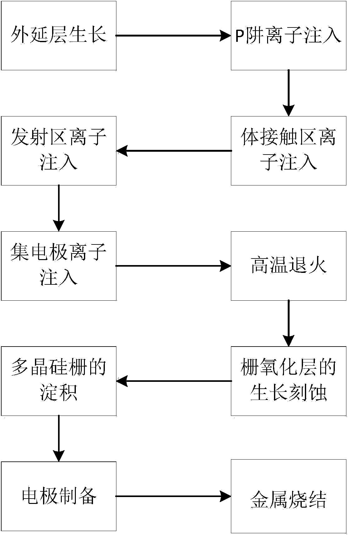
[0031] Step 1: grow epitaxial layer.

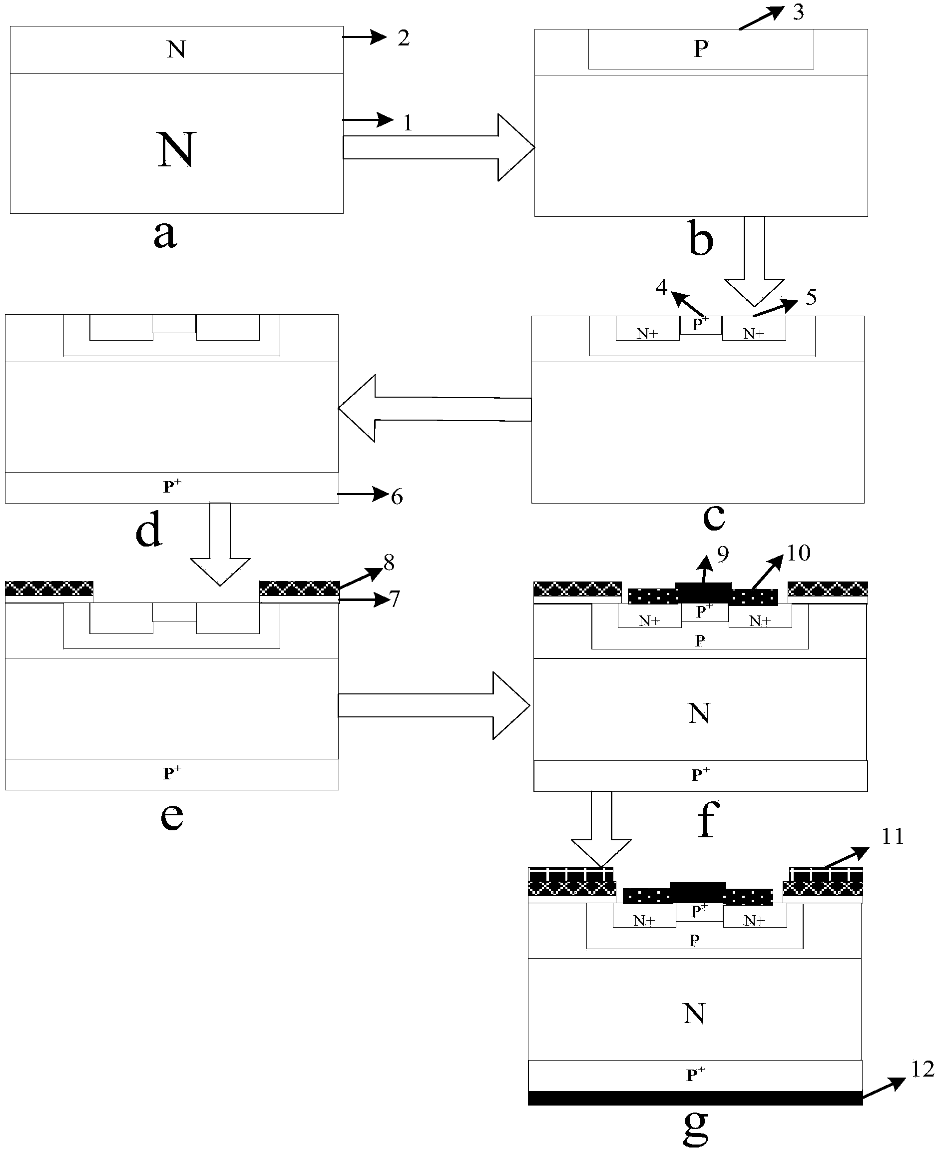
[0032] First perform RCA standard cleaning on the N-type silicon carbide substrate 1, and then epitaxially grow on the entire substrate with a thickness of 0.8 μm and a nitrogen ion doping concentration of 2×10 15 cm -3 N-type epitaxial layer 2, such as image 3 a, The epitaxy process conditions are: temperature 1600°C, pressure 100mbar, silane and propane as reaction gas, pure hydrogen as carrier gas, and liquid nitrogen as dopant source.

[0033] Step 2: P well implantation.

[0034] (2.1) Deposit Al with a thickness of 1.5 μm on the entire silicon carbide epitaxial layer by low-pressure chemical vapor deposition as a barrier layer for P-well ion implantation, and then apply glue and photoetch the P-w...

Embodiment 2

[0057] Example 2: Dislocations in the base plane are 10 4 / cm -3 , the substrate concentration is 3×10 14 cm -3 N-channel silicon carbide insulated gate bipolar transistors were prepared on the micropipe-free N-type SiC substrate.

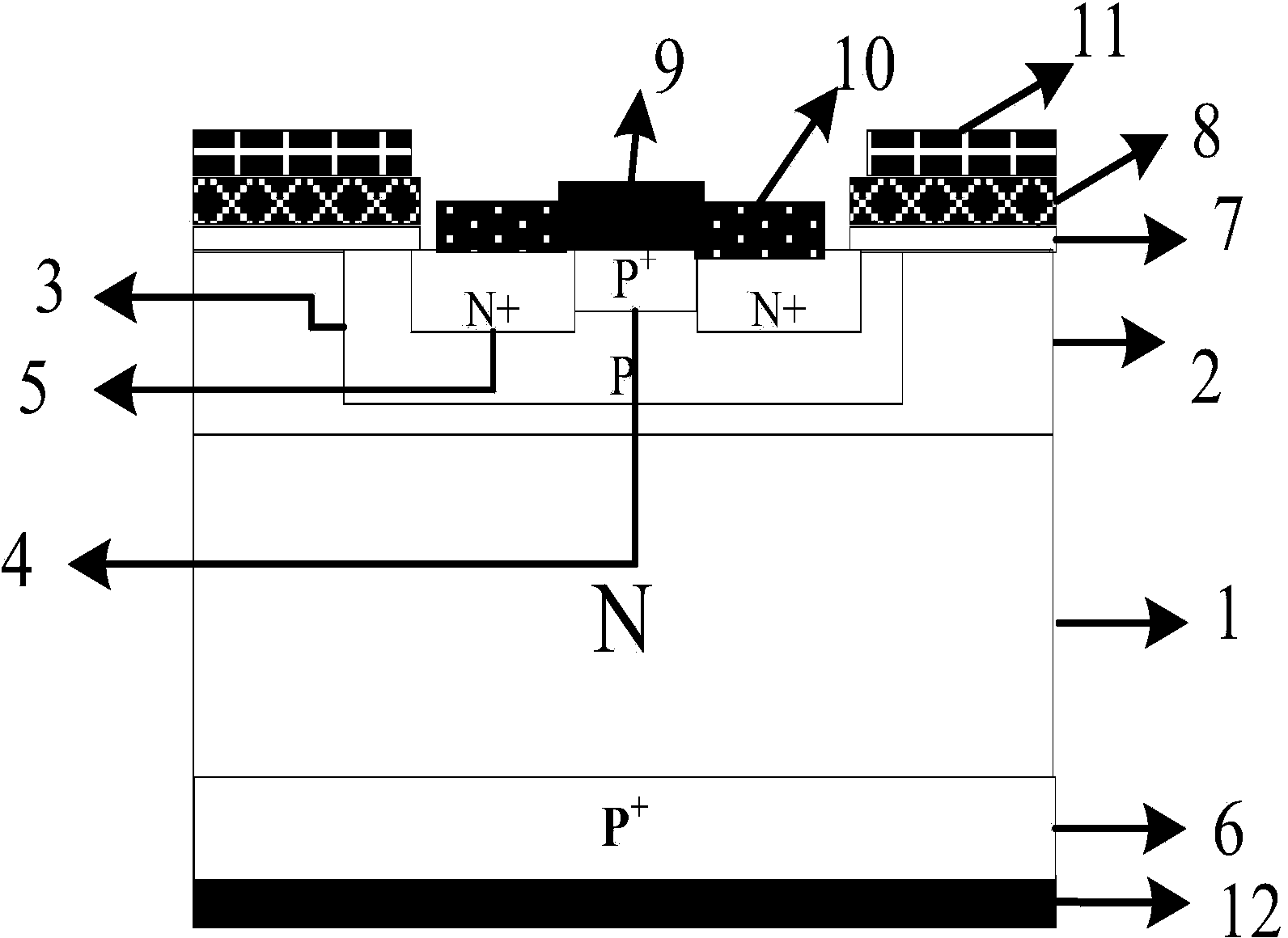
[0058] refer to figure 1 and figure 2 , the implementation steps of this embodiment are as follows:

[0059] Step 1: RCA standard cleaning is performed on the N-type SiC substrate 1 first, and the epitaxial growth thickness on the entire substrate is 1 μm, and the nitrogen ion doping concentration is 5×10 15 cm -3 N-type epitaxial layer 2, such as image 3 a. The process conditions are as follows: temperature is 1600°C, pressure is 100mbar, silane and propane are used as reaction gas, pure hydrogen is used as carrier gas, and liquid nitrogen is used as dopant source.

[0060] The second step: P well injection.

[0061] The specific implementation of this step is the same as step 2 of embodiment 1.

[0062] The third step: apply glue on t...

Embodiment 3

[0072] Dislocations in the basal plane are 10 4 / cm -3 , the substrate concentration is 5×10 14 cm -3 N-channel silicon carbide insulated gate bipolar transistors were prepared on the micropipe-free N-type SiC substrate.

[0073] refer to figure 1 and figure 2 , the implementation steps of this embodiment are as follows:

[0074] Step A: epitaxial layer growth.

[0075] First perform RCA standard cleaning on the N-type silicon carbide substrate 1, and then epitaxially grow the entire substrate with a thickness of 1.4 μm and a nitrogen ion doping concentration of 7×10 15 cm -3 N-type epitaxial layer 2, such as image 3 a, The epitaxy process conditions are: temperature 1600°C, pressure 100mbar, silane and propane as reaction gas, pure hydrogen as carrier gas, and liquid nitrogen as dopant source.

[0076] Step B: P-well implantation.

[0077] The specific implementation of this step is the same as step 2 of embodiment 1.

[0078] Step C: P + Body contact area injec...


PUM

PropertyMeasurementUnit
thicknessaaaaaaaaaa

Abstract

The invention discloses a method for manufacturing an N-channel punch-through silicon carbide insulated gate bipolar transistor. The method mainly solves the problem that currently, the manufacturing cost of the silicon carbide insulated gate bipolar transistor is too high. The method includes the implementation steps that first, an N-type silicon carbide substrate with excellent structural performance is selected, and an N-type epitaxial layer is grown on the front face of the substrate in an epitaxial mode; second, a P well region, a P+ body contact region and an N+ emitter region are sequentially formed on the epitaxial layer of the substrate through ion implantation; third, ion implantation of a P+ collector region and high-temperature annealing are performed on the back face of the substrate, and implanted impurities are activated; fourth, an etching gate oxide layer is grown on the front face of the substrate, and a polysilicon gate is deposited; fifth, metal is deposited on the front face and the back face of the substrate respectively, and electrodes are led out. Compared with an existing method, the method for manufacturing the N-channel silicon carbide insulated gate bipolar transistor has the advantages that an over-thick voltage resisting layer does not need to be grown in an epitaxial mode, a large amount of production cost is saved, the technological steps are simplified, and the transistor can be used for an inverter, a switch power supply and a lighting circuit.

Description

technical field [0001] The invention belongs to the field of microelectronic technology, and relates to a method for preparing a semiconductor device, in particular to a punch-through SiC IGBT using a substrate as a voltage-resistant layer, which can be widely used in frequency converters, inverters, switching power supplies, lighting circuits and motors and other fields. technical background [0002] Silicon carbide insulated gate bipolar transistor, or SiC IGBT, is a new type of high-voltage resistant device developed based on silicon carbide materials. At present, the mainstream solid-state device used in the field of power electronics is Si IGBT, and its turn-off voltage is 0.6-6.5kV. After 30 years of development, Si IGBT has reached the limit of performance and device structure. With the development of new applications such as electric vehicles, photovoltaic and wind energy green energy, and smart grids, a new leap in the performance of power electronic devices is req...

Claims


Application Information

Patent Timeline
Patent Type & Authority Applications(China)
IPC IPC(8): H01L21/28H01L21/331
CPCH01L21/26506H01L29/24H01L29/66068
Inventor 郭辉翟华星宋庆文张艺蒙张玉明汤晓燕
Owner XIDIAN UNIV
Why Eureka
Try Eureka