Preparation method of silicon carbide insulated gate bipolar transistor

A technology of bipolar transistors and insulated gates, which is applied in the fields of inverters, lighting circuits and motors, microelectronics, switching power supplies, and frequency converters. Achieve the effects of saving preparation cost and time, reducing preparation difficulty, saving resources and energy

Active Publication Date: 2016-10-12
XIDIAN UNIV
View PDF2 Cites 0 Cited by
  • Summary
  • Abstract
  • Description
  • Claims
  • Application Information

AI Technical Summary

Problems solved by technology

[0005] 1. High preparation cost
For example, SiC epitaxial equipment is expensive, and the epitaxial process consumes a lot of energy, etc.
[0006] 2. It is technically difficult to grow thicker epitaxial layers
For the growth of epitaxial layers with a thickness of 100 μm and above, the process requirements are high, which can only be achieved by top silicon carbide device companies such as Cree in the world. Therefore, technical bottlenecks limit the popularization and application of high-power SiC IGBTs

Method used


Image

  • Preparation method of silicon carbide insulated gate bipolar transistor
  • Preparation method of silicon carbide insulated gate bipolar transistor

Examples


Embodiment 1

[0025] Example 1: Dislocations in the base plane are 10 4 / cm -3 , the substrate concentration is 2×10 14 cm -3 Silicon carbide insulated gate bipolar transistors were prepared on the micropipe-free P-type SiC substrate.

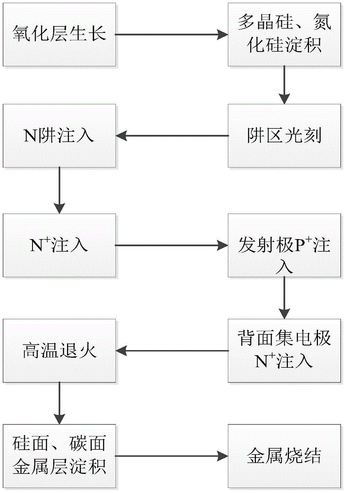
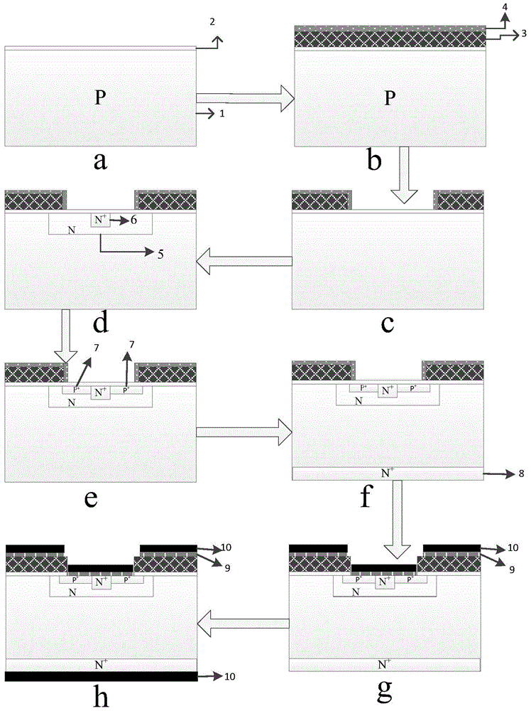
[0026] refer to figure 1 with figure 2 , the implementation steps of this embodiment are as follows:

[0027] Step 1: growing an oxide layer on the silicon surface.

[0028] First dry oxygen oxidation on the silicon surface of the substrate at 1200°C for one hour, and then wet oxygen oxidation at 950°C for one hour to form an oxide layer 2 with a thickness of 50nm on the silicon surface of the substrate, as figure 2 a; then at 1050°C in N 2 Annealing under atmosphere to reduce SiO 2 The roughness of the film surface.

[0029] Step 2: Deposit polysilicon.

[0030] On the oxide layer, a polysilicon 3 with a thickness of 2 μm and a silicon nitride protective layer 4 with a thickness of 100 nm were sequentially deposited by the low-pressure chemical ...

Embodiment 2

[0047] Dislocations in the basal plane are 10 4 / cm -3 , the substrate concentration is 6×10 14 cm -3 Silicon carbide insulated gate bipolar transistors were prepared on the micropipe-free P-type SiC substrate.

[0048] refer to figure 1 with figure 2 , the implementation steps of this embodiment are as follows:

[0049] Step A: growing an oxide layer on the silicon surface.

[0050] Dry oxygen oxidation at 1200°C for 2 hours, and then wet oxygen oxidation at 950°C for one hour to form an oxide layer 2 with a thickness of 70nm, as figure 2 a; then at 1050°C in N 2 Annealing under atmosphere to reduce SiO 2 The roughness of the film surface.

[0051] Step B: Deposit polysilicon.

[0052] On the oxide layer, a low-pressure chemical vapor deposition method is used to deposit polysilicon 3 with a thickness of 4 μm and a silicon nitride protective layer 4 with a thickness of 100 nm at a deposition pressure of 220 Pa and a deposition temperature of 650 ° C, such as fig...

Embodiment 3

[0066] Dislocations in the basal plane are 10 4 / cm -3 , the substrate concentration is 1×10 15 cm -3 Silicon carbide insulated gate bipolar transistors were prepared on the micropipe-free P-type SiC substrate.

[0067] refer to figure 1 with figure 2 , the implementation steps of this embodiment are as follows:

[0068] Step 1: grow the oxide layer on the silicon surface, that is, dry oxygen oxidation on the silicon surface of the substrate at 1200°C for 3 hours, and then wet oxygen oxidation at 950°C for 90 minutes to form an oxide layer with a thickness of 100nm on the silicon surface of the substrate. Layer 2, such as figure 2 a; then at 1050°C in N 2 Annealing under atmosphere to reduce SiO 2 The roughness of the film surface.

[0069] Step 2: On the oxide layer, the polysilicon 3 and the silicon nitride protective layer 4 are sequentially deposited by low-pressure chemical vapor deposition method, and the conditions are as follows: deposition pressure 300Pa, d...


PUM

PropertyMeasurementUnit
thicknessaaaaaaaaaa
thicknessaaaaaaaaaa
thicknessaaaaaaaaaa

Abstract

The invention discloses a preparation method for a silicon carbide insulated gate bipolar transistor. The preparation method mainly solves the problem that the preparation cost of an existing SiC insulated gate bipolar transistor is too high. The preparation method comprises the steps that a P-type SiC substrate with excellent structural performance is selected, an oxide layer is grown on the silicon surface of the substrate, and then polycrystalline silicon and silicon nitride are sequentially formed through deposition; a gate self alignment process is adopted, a well region window is formed in the surface, with the polycrystalline silicon and silicon nitride in a deposition mode, of the substrate in an etching mode, and an N well, an N+ contact area and an emitter electrode region are formed through ion implantation; a collector electrode region is formed in the carbon surface of the substrate through ion implantation; then, high-temperature annealing is conducted, a drive-in process is completed, and implanted impurities are activated; metal layers are formed on the silicon surface and the carbon surface of the substrate through deposition, and all electrodes are led out; finally, metal sintering is conducted, and good contact is formed. Compared with the prior art, the preparation method for the silicon carbide insulated gate bipolar transistor has the advantages that an over-thick voltage-withstanding layer does not need to be grown through an epitaxy technique, the production cost is reduced greatly, processing steps are simplified, and the silicon carbide insulated gate bipolar transistor can be applied to a switched-mode power supply and a lighting circuit.

Description

technical field [0001] The invention belongs to the technical field of microelectronics, relates to a preparation method of a semiconductor device, and can be widely used in the fields of frequency converters, inverters, switching power supplies, lighting circuits, motors and the like. technical background [0002] Looking back at the development of power semiconductor devices, it can be roughly divided into four generations. The first generation is represented by the thyristor SCR that appeared in the 1950s. Its advantage is that the power capacity is particularly large, and the current level has reached 7000V / 8000A. But the disadvantage is that the switching speed is low and the shutdown is uncontrollable. In order to solve the uncontrollable problem of SCR turn-off, the second-generation products represented by gate turn-off thyristor GTO and giant bipolar transistor GTR appeared in the 1970s. They are all self-turn-off devices, the switching speed is higher than that ...

Claims


Application Information

Patent Timeline
Patent Type & Authority Patents(China)
IPC IPC(8): H01L21/331
CPCH01L29/66068
Inventor 郭辉翟华星张艺蒙宋庆文张玉明汤晓燕
Owner XIDIAN UNIV
Why Eureka
Try Eureka