Method for manufacturing TFT array substrate

A manufacturing method and array substrate technology, which are applied in semiconductor/solid-state device manufacturing, optics, instruments, etc., can solve problems such as high cost and complex process flow, and achieve the effect of reducing usage, simplifying process flow, and reducing production cost

Inactive Publication Date: 2014-07-16
TCL CHINA STAR OPTOELECTRONICS TECH CO LTD
View PDF4 Cites 2 Cited by
  • Summary
  • Abstract
  • Description
  • Claims
  • Application Information

AI Technical Summary

Problems solved by technology

In the prior art, no matter whether the amorphous silicon semiconductor process or the metal oxide semiconductor process is adopted, not only the process flow is complicated, but also the cost is high

Method used


Image

  • Method for manufacturing TFT array substrate
  • Method for manufacturing TFT array substrate
  • Method for manufacturing TFT array substrate

Examples


Embodiment Construction

[0046] Preferred embodiments of the present invention will be described below with reference to the accompanying drawings.

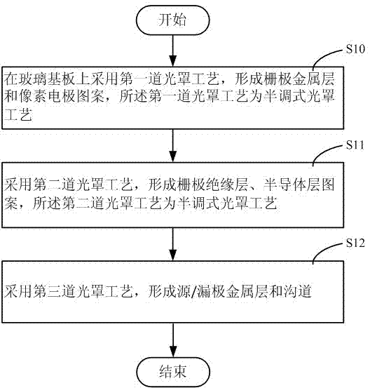
[0047] Such as figure 1 Shown is a schematic diagram of the main flow in an embodiment of a method for manufacturing a TFT array substrate provided by the present invention; in this embodiment, the method is suitable for manufacturing an amorphous silicon array substrate for a flat panel, and the method Including the following steps:

[0048]Step S10, using a first mask process on the glass substrate to form a gate metal layer and a pixel electrode pattern, the first mask process being a half tone mask process;

[0049] Specifically, this step includes:

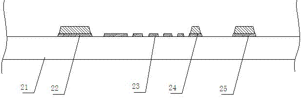
[0050] Deposit a pixel electrode layer and a gate metal layer with a predetermined thickness on the glass substrate, and coat photoresist, for example, in one embodiment, deposit a thickness of 1000 Å to 6000 Å on the glass substrate by sputtering or thermal evaporation. ? gate metal film, and deposi...


PUM


Abstract

The embodiment of the invention discloses a method for manufacturing a TFT array substrate. The method comprises the following steps that a first photomask technology is adopted in a glass substrate to form a grid electrode metal layer and a pixel electrode pattern, and the first photomask technology is a semi-adjustment type photomask technology; a second photomask technology is adopted to form a grid electrode insulating layer and a semiconductor layer pattern, and the second photomask technology is the semi-adjustment type photomask technology or a grey photomask technology; a third photomask technology is adopted to form a source / drain electrode metal layer and a channel. By means of the method, the technological processes for manufacturing an amorphous silicon semiconductor or oxide semiconductor TFT array substrate of a panel display panel are simplified, the using number of mask plates is reduced, and production cost is reduced.

Description

technical field [0001] The invention relates to a manufacturing technology of a flat panel display, in particular to a manufacturing method of a thin film field effect transistor (Thin Film Transistor, TFT) array substrate. Background technique [0002] In recent years, display technology has developed rapidly, and flat-panel displays have replaced bulky CRT displays and are increasingly embedded in people's daily lives. Currently, commonly used flat panel displays include liquid crystal displays (Liquid Crystal Display, LCD) and organic light-emitting diode (Organic Light-Emitting Diode, OLED) displays. The above-mentioned flat-panel display has the characteristics of small size, low power consumption, and no radiation, and occupies a dominant position in the current flat-panel display market. [0003] In the array substrate of a flat panel display, each pixel is equipped with a switching unit for controlling the pixel, that is, a thin film field effect transistor (Thin Fi...

Claims


Application Information

Patent Timeline
IPC IPC(8): H01L21/84H01L21/027
CPCH01L27/1288G02F1/134363G02F1/1368H01L27/1225H01L27/124H01L29/66969H01L29/7869
Inventor 徐向阳
Owner TCL CHINA STAR OPTOELECTRONICS TECH CO LTD
Why Eureka
Try Eureka