Double-color all-optical switch based on quantum well inter-subband transition cavity-induced coherence effect

A coherent effect, all-optical switching technology, applied in semiconductor devices, electrical components, circuits, etc., can solve the problems of large size of resonant cavity and difficult integration, achieve low energy consumption, easy miniaturization and integration, and realize miniaturization and integration. integrated effect

Active Publication Date: 2014-07-16
JILIN UNIV
View PDF7 Cites 2 Cited by
  • Summary
  • Abstract
  • Description
  • Claims
  • Application Information

AI Technical Summary

Problems solved by technology

The existing two-color switch based on the quantum coherence of the atomic system operates in the visible and near-infrared regions, not in the op

Method used


Image

  • Double-color all-optical switch based on quantum well inter-subband transition cavity-induced coherence effect
  • Double-color all-optical switch based on quantum well inter-subband transition cavity-induced coherence effect

Examples


Embodiment 1

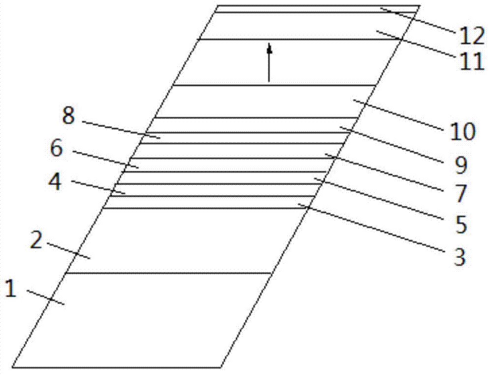
[0020] refer to figure 1 , the substrate 1 is GaAs, followed by an AlAs layer with a thickness of 3900nm; the first barrier layer 3 is composed of Al 0.4 Ga 0.6 As, the thickness is 20nm; the first quantum well layer 4, the composition is Al 0.16 Ga 0.84 As, the thickness is 6.7nm; the second barrier layer 5, the composition is Al 0.4 Ga 0.6 As, the thickness is 4.2nm; the second quantum well layer 6, the composition is Al 0.16 Ga 0.84 As, the thickness is 6.7nm; the third barrier layer 7, the composition is Al 0.4 Ga 0.6 As, with a thickness of 4.2nm; the third quantum well layer 8, composed of GaAs, with a thickness of 7.8nm; the fourth barrier layer 9, composed of Al 0.4 Ga 0.6 As, the thickness is 2.9nm; the continuum 10, the composition is Al 0.16 Ga 0.84 As, the thickness is 160nm. From the first barrier layer 3 to the continuous region 10 is a cycle, and then grow 9 cycles, a total of 10 cycles, and then grow a cover layer 11, the composition is Al 0.4 Ga ...

Embodiment 2

[0022] refer to figure 1 , the substrate 1 is GaAs, followed by an AlAs layer with a thickness of 5000nm; the first barrier layer 3 is composed of Al 0.35 Ga 0.65 As, the thickness is 10nm; the first quantum well layer 4, the composition is Al 0.1 Ga 0.9 As, the thickness is 8nm; the second barrier layer 5, the composition is Al 0.35 Ga 0.65 As, the thickness is 3nm; the second quantum well layer 6, the composition is Al 0.1 Ga 0.9 As, the thickness is 8nm; the third barrier layer 7, the composition is Al 0.35 Ga 0.65 As, the thickness is 3nm; the third quantum well layer 8 is composed of GaAs, and the thickness is 10nm; the fourth barrier layer 9 is composed of Al 0.35 Ga 0.65 As, the thickness is 2nm; the continuum 10, the composition is Al 0.1 Ga 0.9 As, the thickness is 160nm. From the first barrier layer 3 to the continuous region 10 is a cycle, and then grow 14 cycles, a total of 15 cycles, and then grow a cover layer 11, the composition is Al 0.4 Ga 0.6 A...

Embodiment 3

[0024] refer to figure 1 , the substrate 1 is GaAs, followed by an AlAs layer with a thickness of 2000nm; the first barrier layer 3 is composed of Al 04 Ga 0.6 As, the thickness is 30nm; the first quantum well layer 4, the composition is Al 0.2 Ga 0.8 As, the thickness is 1.8nm; the second barrier layer 5, the composition is Al 04 Ga 0.6 As, the thickness is 5nm; the second quantum well layer 6, the composition is Al 0.2 Ga 0.8 As, the thickness is 1.8nm; the third barrier layer 7, the composition is Al 04 Ga 0.6 As, the thickness is 5nm; the third quantum well layer 8 is composed of GaAs, and the thickness is 5.3nm; the fourth barrier layer 9 is composed of Al 04 Ga 0.6 As, the thickness is 4.5nm; the continuum 10, the composition is Al 0.2 Ga 0.8 As, the thickness is 160nm. From the first barrier layer 3 to the continuous region 10 is a period, and then grow 5 periods, a total of 6 periods, and then grow a covering layer 11, the composition is Al 0.4 Ga 0.6 As...


PUM

PropertyMeasurementUnit
Thicknessaaaaaaaaaa
Thicknessaaaaaaaaaa
Thicknessaaaaaaaaaa

Abstract

The invention discloses a double-color all-optical switch based on a quantum well inter-subband transition cavity-induced coherence effect, and belongs to the technical field of semiconductor materials. According to the structure of the double-color all-optical switch, an AlAs layer (2), a first barrier layer (3), a first quantum well layer (4), a second barrier layer (5), a second quantum well layer (6), a third barrier layer (7), a third quantum well layer (8), a fourth barrier layer (9) and a continuous area (10) sequentially grow on a substrate (1) made of GaAs materials, a cycle is from the first barrier layer (3) to the continuous area (10), six to fifteen cycles are arranged, and then a covering layer (11) and an air isolation layer (12) are provided. The double-color all-optical switch based on the quantum well inter-subband transition cavity-induced coherence effect can work at a medium-far infrared wave band, serves as a complete band gap switch of an infrared radiation source with low energy consumption and high efficiency, and has application value on the aspects of satellite detection and communication. The structure and materials of the double-color all-optical switch can be selected artificially, and the double-color all-optical switch has the advantages of easily achieving a wide wave band, miniaturization and integration.

Description

technical field [0001] The invention belongs to the technical field of semiconductor materials, in particular to a two-color all-optical switch based on the cavity-induced coherence effect of quantum well sub-band transitions. Background technique [0002] Optical switches are optoelectronic devices used for physical conversion and logic operations on optical transmission or optical integrated circuits. The dual-color optical switch involved in the invention can be used for physical or logical control of multi-wavelength optical paths, and is an important application in the field of optical information processing and processing. The existing two-color switch based on the quantum coherence of the atomic system operates in the visible and near-infrared regions, not in the optical communication band, and the size of the resonant cavity is relatively large, so it is not easy to integrate with optical integrated circuits. The invention is based on the quantum coherence effect of...

Claims


Application Information

Patent Timeline
IPC IPC(8): H01L31/08
CPCH01L31/035236H01L31/111
Inventor 王涛苏雪梅
Owner JILIN UNIV
Why Eureka
Try Eureka