Thin film transistor array substrate, manufacturing method and liquid crystal display panel

A technology of thin film transistors and array substrates, which is applied in the field of liquid crystal display, and can solve problems such as lowered display quality of liquid crystal display panels, uneven color of liquid crystal display panels, and image deformation.

Active Publication Date: 2014-07-23
SHANGHAI AVIC OPTOELECTRONICS +1
View PDF7 Cites 11 Cited by
  • Summary
  • Abstract
  • Description
  • Claims
  • Application Information

AI Technical Summary

Problems solved by technology

The distance between the two substrates is not equal, resulting in defects such as uneven color and image defor

Method used


Image

  • Thin film transistor array substrate, manufacturing method and liquid crystal display panel
  • Thin film transistor array substrate, manufacturing method and liquid crystal display panel
  • Thin film transistor array substrate, manufacturing method and liquid crystal display panel

Examples


no. 1 example

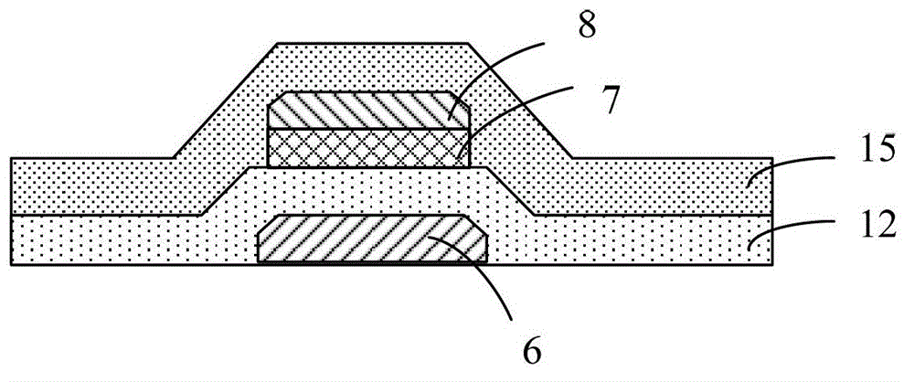
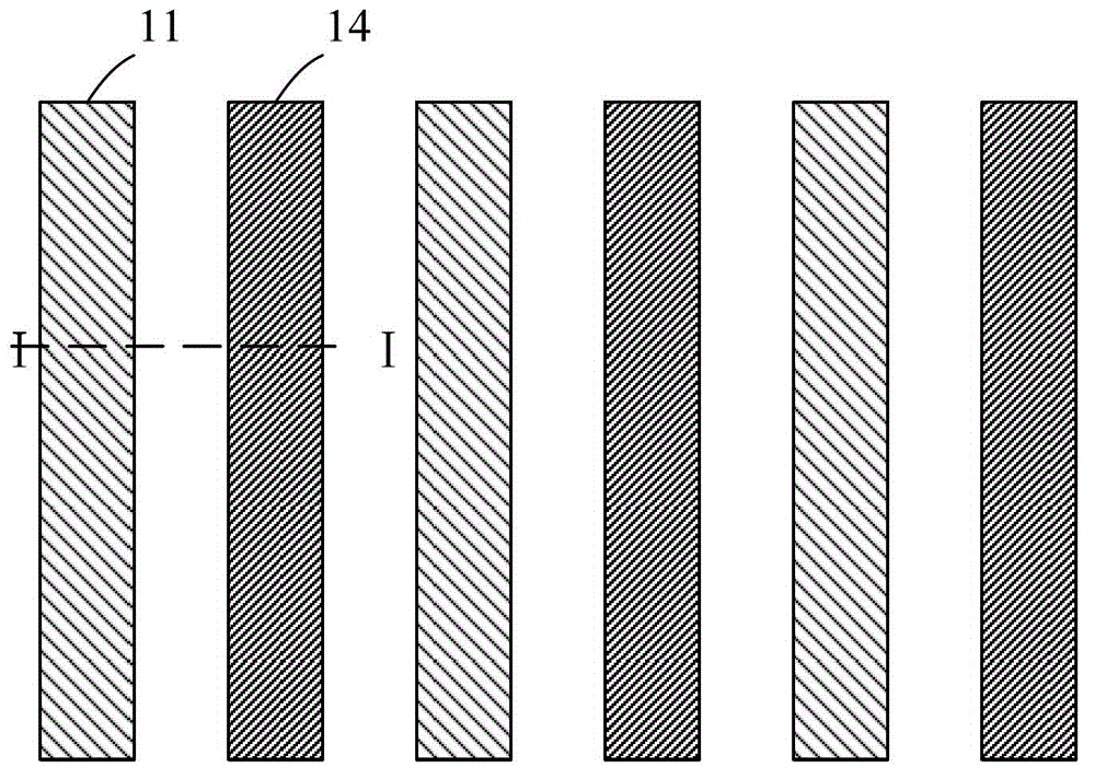
[0047] The data line leads are divided into a plurality of first data line leads located under the insulating layer and a plurality of second data line leads located on the insulating layer that do not overlap with the positions of the first data lead wires; The wire lead is composed of a first metal layer, and the second data line lead is composed of a second metal layer; the lead film layer at the position of the second data line lead includes the first sub-increasing layer, the second sub-increasing layer .

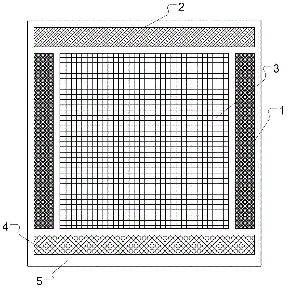
[0048] refer to Figure 8 , Figure 8 It is a schematic cross-sectional view of the film layer of the data line lead area 4 in the first embodiment of the present invention. The array substrate of the liquid crystal display device provided by the present invention includes a plurality of first data line leads 11 and second data line leads 14 arranged at intervals along the same direction, such as image 3 As shown, the distance between the leads of two adjacent data...

no. 2 example

[0059] The thin film transistor array substrate also includes a common electrode line lead area, and the common electrode line is divided into a plurality of first common electrode line leads located under the insulating layer and a plurality of second common electrodes located on the insulating layer Wire. The first common electrode lead is made of a first metal layer, and the second common electrode lead is made of a second metal layer. On the basis of the first embodiment, a booster layer can also be provided at the lead of the first common electrode line to achieve the purpose of reducing the difference in film layer height on the non-display area around the array substrate. The lead film layer where the first common electrode lead 9 is located includes a third sub-buildup layer and a fourth sub-buildup layer.

[0060] refer to Figure 10 , Figure 10 It is a schematic cross-sectional view of the film layer in the lead area 2 of the common electrode line in the second e...

no. 3 example

[0070] The thin film transistor array substrate also includes a common electrode line lead area, and the common electrode line is divided into a plurality of first common electrode line leads located under the insulating layer and a plurality of second common electrodes located on the insulating layer Wire. The first common electrode lead is made of a first metal layer, and the second common electrode lead is made of a second metal layer. On the basis of the first embodiment, a booster layer can also be provided at the lead of the second common electrode line to achieve the purpose of reducing the difference in film layer height on the non-display area around the array substrate. The lead film layer where the first common electrode lead 9 is located includes a fifth sub-buildup layer and a sixth sub-buildup layer.

[0071] refer to Figure 11 , Figure 11 It is a schematic cross-sectional view of the film layer in the lead area 2 of the common electrode line in the third em...


PUM

PropertyMeasurementUnit
Film thicknessaaaaaaaaaa

Abstract

The invention provides an array substrate used for a liquid crystal display device. A display region is located at the center of the array substrate and a non-display region is arranged all around the display region. The non-display region comprises a gate driver region, a data line lead region and a public electrode line lead region; lead film layers are formed in the data line lead region and the public electrode line lead region, each lead film layer comprises a first metal layer, an insulating layer, a second metal layer and a passivation layer and further comprises one or more height increasing layers, and the height increasing layers, the first metal layers, the insulating layers, the second metal layers and the passivation layers are overlapped. According to the array substrate of the liquid crystal display device, the height increasing layers are arranged in the lead film layers, so that the height difference of the non-display region all around the array substrate is reduced or eliminated, and the quality of display frames of a liquid crystal display is improved.

Description

technical field [0001] The invention relates to the field of liquid crystal display, in particular to a thin film transistor array substrate, a liquid crystal display panel including the thin film transistor array substrate and a manufacturing method of the thin film transistor array substrate. Background technique [0002] Flat-panel displays are currently the mainstream displays, and liquid crystal displays are widely used in electronic products such as computer screens, mobile phones, personal digital assistants, and flat-screen TVs because of their thin and light appearance, power saving, and no radiation. [0003] A liquid crystal display includes a liquid crystal panel, and generally a liquid crystal panel is composed of an array substrate, a color filter substrate, and liquid crystal encapsulated between the two substrates. In the past, a driver chip made of silicon wafers was usually externally connected to the array substrate, but now, the technology of directly int...

Claims


Application Information

Patent Timeline
IPC IPC(8): G02F1/1362G02F1/1368H01L27/12H01L21/77
Inventor 梁艳峰
Owner SHANGHAI AVIC OPTOELECTRONICS
Why Eureka
Try Eureka