Check patentability & draft patents in minutes with Patsnap Eureka AI!

Fin field effect transistor and forming method thereof

A fin-type field effect and transistor technology, which is applied in semiconductor devices, semiconductor/solid-state device manufacturing, electrical components, etc., can solve the problems of complex process and high cost of multi-threshold voltage transistors, and achieve the effect of low cost and simple process

Active Publication Date: 2014-07-23
SEMICON MFG INT (SHANGHAI) CORP
View PDF5 Cites 9 Cited by
  • Summary
  • Abstract
  • Description
  • Claims
  • Application Information

AI Technical Summary

Problems solved by technology

[0006] The problem solved by the present invention is that the process of forming multi-threshold voltage transistors in the prior art is complex and costly

Method used


Image

  • Fin field effect transistor and forming method thereof
  • Fin field effect transistor and forming method thereof
  • Fin field effect transistor and forming method thereof

Examples


Embodiment Construction

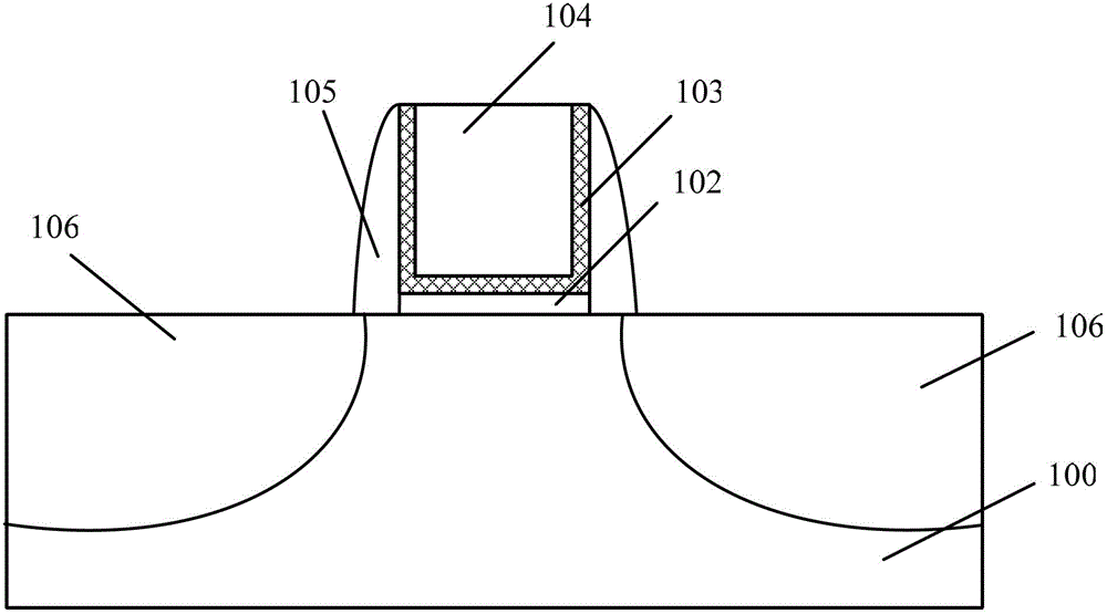
[0033] It can be seen from the background art that in the prior art, the process of forming the fin field effect transistor with multiple threshold voltages is complicated and the cost is high.

[0034] The inventors of the present invention have studied the formation method of a fin field effect transistor with a negative cover region (Underlap), and found that because the negative cover region is not subjected to lightly doped drain implantation (LDD) and halo implantation (Halo Implantation), the The above-mentioned negative covering region can increase the width of the effective channel region of the fin field effect transistor and alleviate the short channel effect. Moreover, the widths of different negative cover regions have different influences on the electric field distribution in the channel region of the fin field effect transistor, and have different effects on the threshold voltage. Therefore, fin field effects with different threshold voltages can be obtained by c...


PUM


Abstract

Disclosed are a fin field effect transistor and a forming method thereof. The forming method of the fin field effect transistor comprises: providing a semiconductor substrate, the semiconductor substrate being provided with a first area and a second area, the first area and the second area being provided with projection fin portions and grid structures disposed on the fin portions; forming first side walls at the two sides of the gate structures of the first area, a part of the fin portions covered by the first side walls constituting a first negative covering area; forming second side walls at the two sides of the grid structures of the second area, the width of the second side walls being smaller than the width of the first side walls, a part of the fin portions covered by the second side walls constituting a second negative covering area; and performing ion implantation on the fin portions at the two sides of the grid structures of the first area and the second area, and forming a source area and a drain area. According to the forming method of the fin field effect transistor, fin field effect transistors with different threshold voltages can be formed, and the process is simple.

Description

technical field [0001] The invention relates to the technical field of semiconductors, in particular to a fin field effect transistor and a forming method thereof. Background technique [0002] With the advancement of integrated circuit technology, the integration level of the chip is getting higher and higher, and the scale is getting larger and larger, but the power consumption of the chip is also increasing. A single chip usually includes a core logic transistor area and an input / output (I / O) transistor area. The threshold voltage of the core logic transistor is low to reduce system power consumption, and the threshold voltage of the input / output transistor is high to ensure high drive capability and breakdown voltage. Therefore, how to obtain transistors with different threshold voltages on a single chip has become the focus of research. [0003] Please refer to figure 1 , is a schematic structural diagram of a MOS transistor in the prior art, including: a semiconduct...

Claims


Application Information

Patent Timeline
Patent Type & Authority Applications(China)
IPC IPC(8): H01L21/336H01L29/78H01L29/423
CPCH01L29/0603H01L29/1033H01L29/4232H01L29/66795H01L29/785
Inventor 三重野文健殷华湘
Owner SEMICON MFG INT (SHANGHAI) CORP
Features
  • R&D
  • Intellectual Property
  • Life Sciences
  • Materials
  • Tech Scout
  • Unparalleled Data Quality
  • Higher Quality Content
  • 60% Fewer Hallucinations
Learn More