Fabrication method of top metal interconnection layer

A top-layer metal and manufacturing method technology, applied in semiconductor/solid-state device manufacturing, electrical components, circuits, etc., can solve problems such as collapse, affecting wafer curvature, semiconductor device fracture, etc., to avoid grain size increase and improve mechanical resistance. Pressure, the effect of improving product yield

Active Publication Date: 2016-07-27
SEMICON MFG INT (SHANGHAI) CORP
View PDF5 Cites 0 Cited by
  • Summary
  • Abstract
  • Description
  • Claims
  • Application Information

AI Technical Summary

Problems solved by technology

Usually, after the annealing process, the lattice of the top metal interconnect layer changes, thereby increasing the grain size (GrainSize), and the grain size even reaches 2 μm or more, causing deformation of the semiconductor device, that is, affecting the curvature of the entire wafer, Excessive changes in the curvature of the wafer will affect the mechanical stress of the top metal interconnection layer, resulting in problems such as fracture and collapse of semiconductor devices during the chemical mechanical polishing process

Method used


Image

  • Fabrication method of top metal interconnection layer
  • Fabrication method of top metal interconnection layer
  • Fabrication method of top metal interconnection layer

Examples


Embodiment Construction

[0018] In order to make the content of the present invention clearer and easier to understand, the content of the present invention will be further described below in conjunction with the accompanying drawings. Of course, the present invention is not limited to this specific embodiment, and general replacements known to those skilled in the art are also covered within the protection scope of the present invention.

[0019] Secondly, the present invention is described in detail by means of schematic diagrams. When describing the examples of the present invention in detail, for the convenience of explanation, the schematic diagrams are not partially enlarged according to the general scale, which should not be used as a limitation of the present invention.

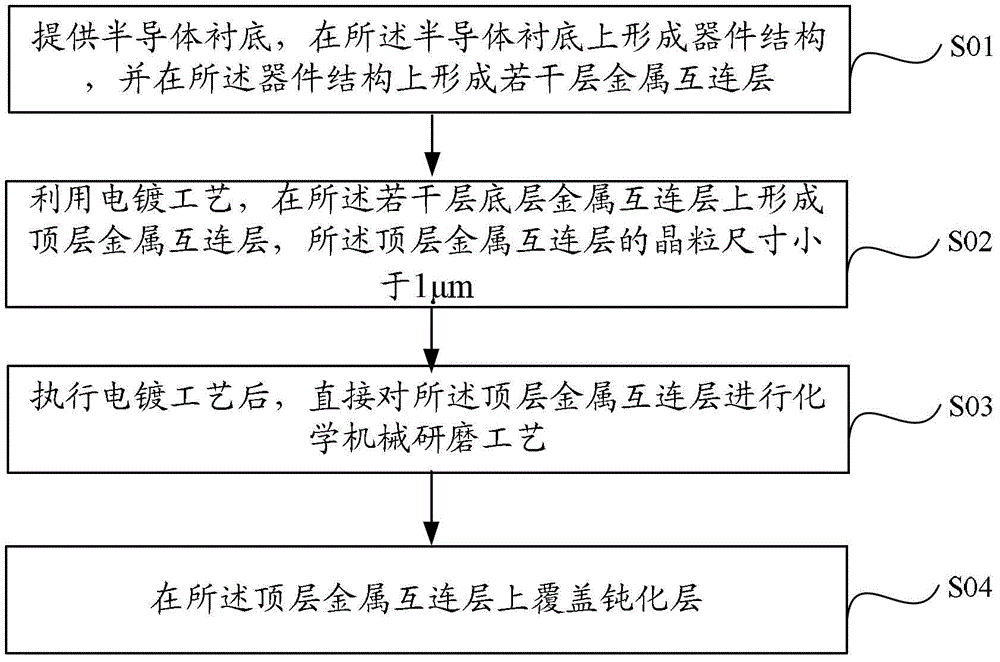
[0020] figure 1 It is a schematic flowchart of the manufacturing process of the top metal interconnection layer in an embodiment of the present invention. Such as figure 1 As shown, the present invention provides a method f...


PUM

PropertyMeasurementUnit
particle sizeaaaaaaaaaa
thicknessaaaaaaaaaa
thicknessaaaaaaaaaa

Abstract

The invention provides a method for manufacturing top layer metal interconnection layers. The method includes the steps that a semiconductor substrate is provided, a device structure is formed on the semiconductor substrate, and a plurality of bottom layer metal interconnection layers are formed on the device structure; the top layer metal interconnection layers are formed on the multiple bottom layer metal interconnection layers through the electroplating technology, and the grain size of the top layer metal interconnection layers is smaller than 1 micron; next, the chemical and mechanical polishing technology is directly performed on the top layer metal interconnection layers; the top layer metal interconnection layers are covered with passivation layers. Through the method for manufacturing the top layer metal interconnection layers, increase of the grain size of the top layer metal interconnection layers can be avoided, the grain size is controlled to be smaller than 1 micron, and therefore while the wafer conduction test pass percent of semiconductor devices is kept, it is guaranteed that in the chemical and mechanical polishing technology process, the mechanical compressive resistance of the top layer metal interconnection layers is improved, problems such as fracture and collapse occurring to the semiconductor devices are avoided, and the yield of the product is further improved.

Description

technical field [0001] The invention relates to a method for manufacturing a semiconductor device, in particular to a method for manufacturing a top metal interconnection layer. Background technique [0002] In the traditional semiconductor manufacturing process, the top metal interconnect layer (TopMetal) is an indispensable part. With the development of related fields, the requirements for inductance devices are gradually increasing, that is, they need to have a better quality factor Q value, because Reducing the resistivity of the top metal interconnect layer can increase the Q value, and reducing the resistivity of the top metal interconnect layer is generally achieved by thickening the top metal interconnect layer. The thickness of the layer has made higher requirements, and even the top metal interconnection layer with a thickness of 10 μm will be required. [0003] In the prior art, the formation process of the top-level metal interconnection layer usually includes t...

Claims


Application Information

Patent Timeline
Patent Type & Authority Patents(China)
IPC IPC(8): H01L21/768
CPCH01L21/76838H01L21/7684
Inventor 李广宁
Owner SEMICON MFG INT (SHANGHAI) CORP
Why Eureka
Try Eureka