Interconnection structure and manufacture method thereof

A technology of interconnection structure and manufacturing method, which is applied in semiconductor/solid-state device manufacturing, semiconductor/solid-state device parts, semiconductor devices, etc., can solve the problems of complex wiring, increase of wiring resources, damage, etc., to improve device signal accuracy, Effects of reducing wiring noise and simplifying complexity

Inactive Publication Date: 2014-07-23
INST OF MICROELECTRONICS CHINESE ACAD OF SCI
View PDF8 Cites 7 Cited by
  • Summary
  • Abstract
  • Description
  • Claims
  • Application Information

AI Technical Summary

Problems solved by technology

However, these four methods face greater difficulties at the nanoscale, or will reduce the performance parameters of the chip.
Inserting a buffer in a high-speed circuit will damage and reduce the operating frequency of the chip, changing the wiring spacing, adopting twice the wiring spacing and changing the size of the gate circuit will increase the occupied wiring resources, and the traditional shielding of the victim node will make the wiring more complicated. , it is more difficult to use ordinary EDA tools for wiring, and it also increases the cycle and cost of research and development
[0004] At the same time, there will be electromigration when using traditional metal wires

Method used


Image

  • Interconnection structure and manufacture method thereof
  • Interconnection structure and manufacture method thereof
  • Interconnection structure and manufacture method thereof

Examples


Embodiment Construction

[0023] The features and technical effects of the technical solution of the present invention will be described in detail below with reference to the accompanying drawings and in conjunction with schematic embodiments, and an interconnection structure and a manufacturing method thereof that can effectively reduce wiring noise of small-sized devices are disclosed. It should be pointed out that similar reference numerals represent similar structures, and the terms "first", "second", "upper", "lower" and the like used in this application can be used to modify various device structures or process steps . These modifications do not imply spatial, sequential or hierarchical relationships of the modified device structures or process steps unless otherwise specified.

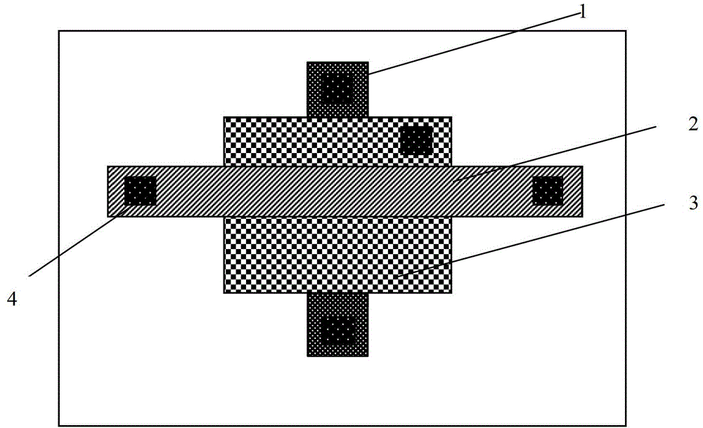
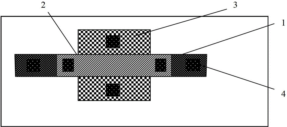
[0024] Figure 1a shows a top view of an interconnection structure according to the present invention, wherein upper and lower interconnection lines are staggered; Figure 1b A top view of an interconnection structure a...


PUM


Abstract

The invention discloses an interconnection structure. The interconnection structure comprises a lower wiring structure which is located on a substrate, a shielding layer which is located on the lower wiring structure, and an upper wiring structure which is located on the shielding layer, wherein the shielding layer comprises grapheme. According to the interconnection structure and a manufacture method thereof, which are provided by the invention, the grapheme which is a single crystal thin conductive material is used as the shielding layer between upper and lower metal connecting lines; the connecting line noise of a small size device is effectively reduced; and the signal accuracy of the device is improved.

Description

technical field [0001] The invention relates to an interconnect structure and a manufacturing method thereof, in particular to a back-end process using single-layer or multi-layer graphene and a manufacturing method thereof. Background technique [0002] As integrated circuits enter the nanoscale range, the crosstalk between the back-end interconnect lines has become one of the important factors that plague circuit design. Crosstalk is the coupling between two signal lines, the mutual inductance and mutual capacitance between the signal lines cause noise on the line. Inductive noise generated by crosstalk can affect signal integrity and chip performance in many ways. For example, when the victim signal is in steady state 0 or steady state 1, glitch interference will be generated. Usually the signal transition time in the circuit is much shorter than the steady-state time, because most signals are often in a steady state, and the glitch noise will destroy this steady state. ...

Claims


Application Information

Patent Timeline
Patent Type & Authority Applications(China)
IPC IPC(8): H01L23/522H01L23/552H01L21/768
Inventor 聂鹏飞粟雅娟朱慧珑赵超贾昆鹏杨杰
Owner INST OF MICROELECTRONICS CHINESE ACAD OF SCI
Why Eureka
Try Eureka