Composite patterned substrate and preparation method thereof

A composite patterning and patterning technology, applied in electrical components, circuits, semiconductor devices, etc., can solve the problems of difficult growth, reducing the efficiency of MOCVD, and difficult nucleation.

Inactive Publication Date: 2014-07-30
项永昌
View PDF4 Cites 15 Cited by
  • Summary
  • Abstract
  • Description
  • Claims
  • Application Information

AI Technical Summary

Problems solved by technology

However, there is a 14% lattice mismatch rate between the sapphire substrate and GaN, which makes it difficult to nucleate and grow. In order to overcome the problem of difficult nucleation, after the substrate is baked at about 1000 ° C, the general treatment method for epitaxy is to grow a layer of thickness 20-40nm poor-quality low-temperature buffer layer, and then turn to high-temperature 3D growth of high-quality GaN. There is high-low temperature conversion in this process, which will reduce the efficiency of MOCVD and the lattice mismatch rate between GaN and the substrate. There are many high-line dislocations, and the temperature difference between different layers is large, resulting in the stress between different layers affecting the crystal performance.

Method used


Image

  • Composite patterned substrate and preparation method thereof
  • Composite patterned substrate and preparation method thereof
  • Composite patterned substrate and preparation method thereof

Examples


Embodiment Construction

[0029] Embodiment of the preparation method of the composite patterned substrate of the present invention: it comprises:

[0030] Step (1), the step of preparing a sapphire patterned substrate; specifically:

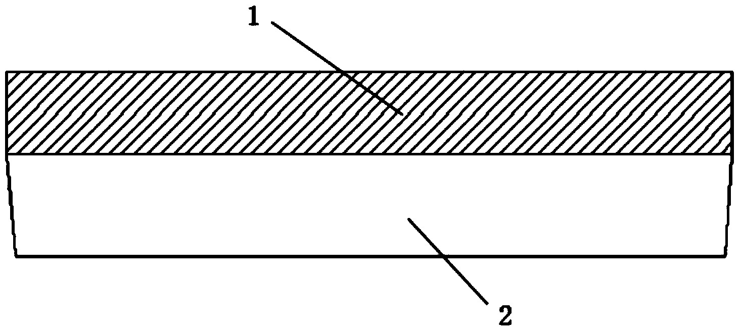
[0031] Step (1.1), uniform photoresist, such as figure 1 As shown, a layer of photoresist 1 with a thickness of 1.5-3.5um is evenly coated on the sapphire flat sheet 2. This thick bottom will directly affect the height of the sapphire pattern etched by ICP when it is etched by ICP later;

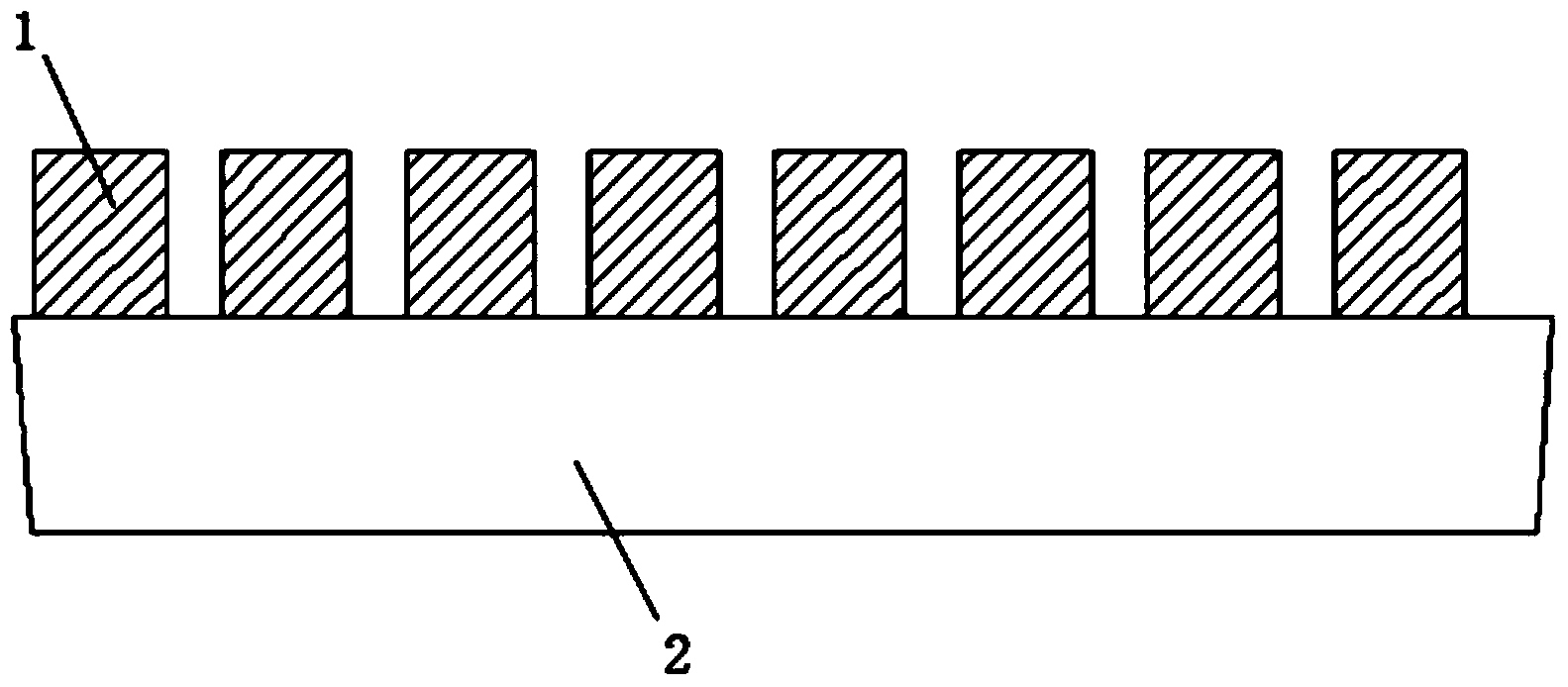
[0032] Step (1.2), exposure and development: use a stepping exposure machine (stepper) to expose the wafer that has evened the photoresist 1, and use the developing solution to develop the exposed film after the exposure is completed. The developed wafer is as follows: figure 2 shown;

[0033] Step (1.3), film hardening treatment: place the developed wafer with photoresist pattern on a hot plate at 90-150°C for 2min-5min to harden the film, let the solvent in the photoresist volati...


PUM

PropertyMeasurementUnit
thicknessaaaaaaaaaa
thicknessaaaaaaaaaa

Abstract

The invention relates to a composite patterned substrate and a preparation method thereof. The composite patterned substrate comprises a sapphire wafer. The maximum ratio of the diameter of circumcircles of the root portions of patterns of the surface of the wafer to the distance between two adjacent pattern central points is 0.95. The surfaces of the upper portions of the patterns are exposed. AlN layers with the thickness ranging from 15 nm to 35 nm are deposited between the root portions of the patterns. According to the composite patterned substrate and the preparation method of the composite patterned substrate, the advantages of the sapphire patterned substrate are reserved; in addition, the AlN layer which is in low lattice mismatching with GaN materials is introduced below the patterned substrate, and the GaN nucleation quality of the substrate in the later using process is effectively improved, so that the GaN growth quality is improved; moreover, the using efficiency of MOCVD can be effectively improved, and productivity is improved.

Description

technical field [0001] The invention belongs to the field of light-emitting diodes, and in particular relates to a multi-layer composite LED patterned substrate of light-emitting diodes and a preparation method thereof. Background technique [0002] Now mainstream LEDs use patterned substrates for epitaxial growth, such as Figure 9 , 10 As shown, on the one hand, the surface pattern provides a variety of growth crystal phase options for later GaN growth, making GaN change from traditional two-dimensional growth to three-dimensional growth, thereby effectively reducing the dislocation density in GaN-based LED materials and avoiding cracks On the other hand, because the array pattern structure increases the scattering of light, changes the optical circuit of the LED, forms diffuse reflection, and improves the light extraction efficiency. However, there is a 14% lattice mismatch rate between the sapphire substrate and GaN, which makes it difficult to nucleate and grow. In ord...

Claims


Application Information

Patent Timeline
Patent Type & Authority Applications(China)
IPC IPC(8): H01L33/20H01L33/00
CPCH01L33/20H01L33/0066H01L33/0075
Inventor 项永昌葛久志
Owner 项永昌
Why Eureka
Try Eureka