Supercharge Your Innovation With Domain-Expert AI Agents!

Low power consumption SRAM (Static Random Access Memory) unit circuit structure

A unit circuit and low power consumption technology, which is applied in the field of low power consumption SRAM unit circuit structure, can solve the problems of reducing static noise margin, chip working voltage, and working voltage not too low, so as to reduce working power consumption, The effect of reducing the driving capability and simplifying the related circuit design

Active Publication Date: 2014-08-06
SUZHOU WULI INFORMATION TECH
View PDF3 Cites 6 Cited by
  • Summary
  • Abstract
  • Description
  • Claims
  • Application Information

AI Technical Summary

Problems solved by technology

[0005] The existing SRAM unit composed of 6 MOSs, when writing, the Pass gate connected to WL will compete with the pull-up PMOS, when reading, WL is turned on, and the transmission tube will form a partial voltage with the pull-down tube to make "0" The higher the value, the lower the static noise margin, which makes the operating voltage of the traditional 6T SRAM not too low, which is the bottleneck of reducing the operating voltage of the entire chip and the bottleneck of reducing power consumption.

Method used


Image

  • Low power consumption SRAM (Static Random Access Memory) unit circuit structure
  • Low power consumption SRAM (Static Random Access Memory) unit circuit structure
  • Low power consumption SRAM (Static Random Access Memory) unit circuit structure

Examples


Embodiment Construction

[0020] The present invention will be described in detail below with reference to the accompanying drawings and in combination with embodiments.

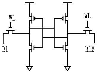
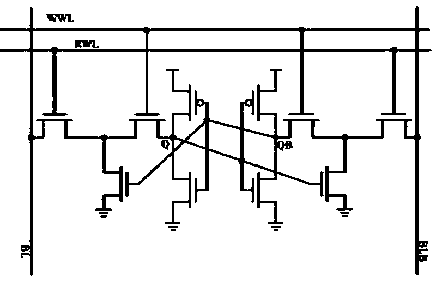
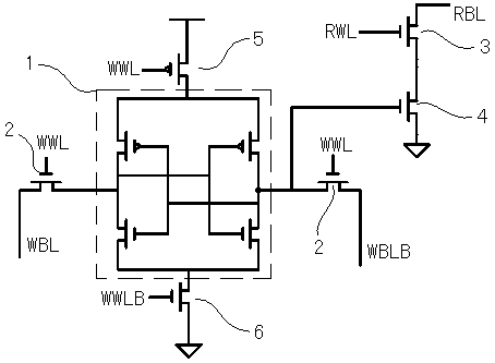
[0021] refer to image 3 As shown, a low-power SRAM unit circuit structure includes a latch 1 composed of four MOS transistors, the two sides of the latch 1 are gate control transistors 2, and one end of the latch 1 passes through a write word line transistor 5 is connected to the power supply, the gate of the word line transistor 5 is connected to the write word line WWL, the other end of the latch 1 is grounded through an inverse signal transistor 6, and the gate of the signal transistor 6 is connected to the inverse signal WWLB of the write word line WWL.

[0022] It also includes a first reading tube 3 and a second reading tube 4, the second reading tube 4 is grounded, and the gate of the second reading tube 4 is connected to the gate control tube 2 and the latch 1 on the one side The gate of the first read transistor is connect...


PUM


Abstract

The invention discloses a low power consumption SRAM (Static Random Access Memory) unit circuit structure which comprises a latch composed of four MOS (Metal Oxide Semiconductor) pipes. Gating pipes are arranged on the two sides of the latch, one end of the latch is connected with a power supply through a writing spool, and the other end of the latch is grounded through an inverted signal pipe. Reading to stored data can be accomplished through two additional pull-down pipes. The circuit in the invention is simple and easy to control. The working voltage of the entire circuit can be lowered to be the same as that of a common digital logic circuit, so that the work power consumption is lowered greatly. Requirements on the driving capability of the SRAM writing circuit are lowered, and related circuit design is simplified. Requirements to a sense amplifier of an SRAM reading circuit are lowered, and the related circuit design is simplified.

Description

technical field [0001] The invention relates to the field of static memory, in particular to a low power consumption SRAM unit circuit structure. Background technique [0002] The static memory (SRAM) in the CMOS integrated circuit process is generally composed of 6 tubes. This structure has a small area, but because this unit will be disturbed when reading and writing, it puts forward higher requirements on the working voltage. , has become a difficulty in reducing the operating voltage and power consumption in the integrated circuit SOC. [0003] refer to figure 1 As shown, the most common SRAM storage unit is composed of 6 MOS, WL represents the word line, and BL / BLB represents the bit line. When reading, WL is turned on, and the bit line whose storage terminal is "0" will be pulled down slowly. When the voltage difference between BL and BLB reaches a certain value, the sense amplifier will read out the data. This memory cell will have some interference and contention ...

Claims


Application Information

Patent Timeline
IPC IPC(8): G11C11/413
Inventor 张建杰张泳培
Owner SUZHOU WULI INFORMATION TECH
Features
  • R&D
  • Intellectual Property
  • Life Sciences
  • Materials
  • Tech Scout
  • Unparalleled Data Quality
  • Higher Quality Content
  • 60% Fewer Hallucinations
Learn More