Narrow trench manufacturing method

A fabrication method and trench technology, applied in semiconductor/solid-state device manufacturing, electrical components, circuits, etc.

Inactive Publication Date: 2014-08-06
SHANGHAI HUALI MICROELECTRONICS CORP
View PDF4 Cites 4 Cited by
  • Summary
  • Abstract
  • Description
  • Claims
  • Application Information

AI Technical Summary

Problems solved by technology

[0003] However, although there is a certain selectivity during dry etching (mainly

Method used


Image

  • Narrow trench manufacturing method
  • Narrow trench manufacturing method
  • Narrow trench manufacturing method

Examples


Embodiment Construction

[0016] In order to make the content of the present invention clearer and easier to understand, the content of the present invention will be described in detail below in conjunction with specific embodiments and accompanying drawings.

[0017] Figure 5 to Figure 9 Each step of the method for fabricating a narrow trench according to a preferred embodiment of the present invention is schematically shown.

[0018] Specifically, such as Figure 5 to Figure 9 As shown, the narrow trench fabrication method according to a preferred embodiment of the present invention includes:

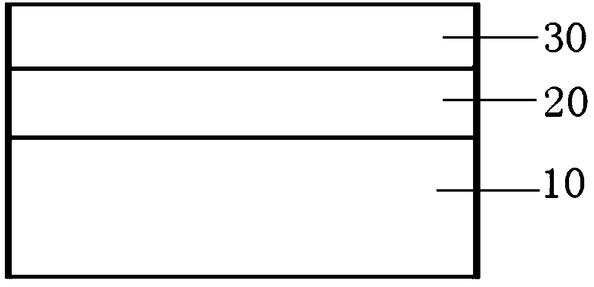
[0019] The first step is for sequentially arranging a silicon nitride layer 2 and a hard mask 3 on a semiconductor substrate 1;

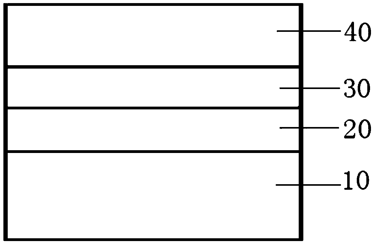
[0020] The second step is for arranging photoresist 4 on hard mask 3;

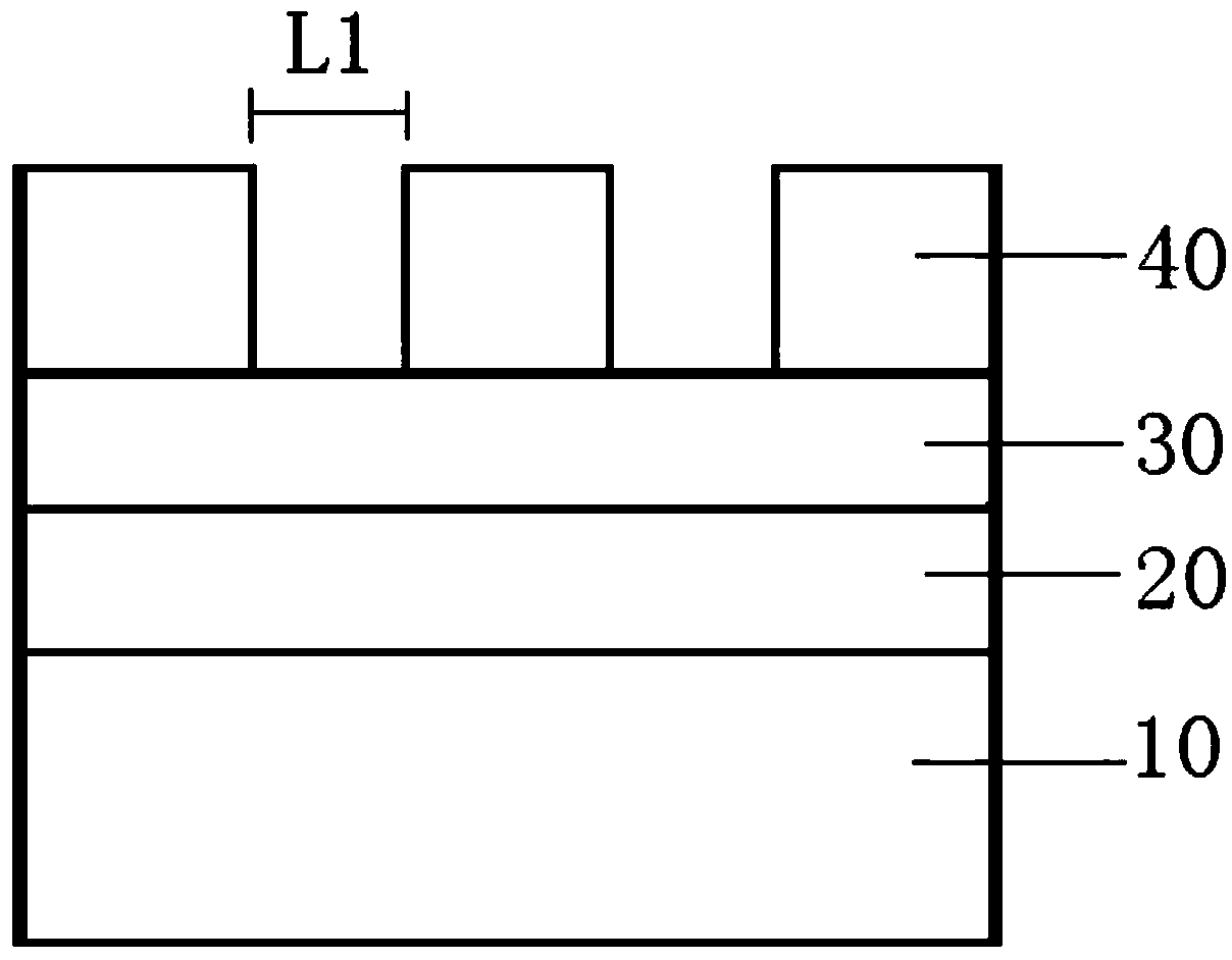
[0021] The third step is to expose and develop the photoresist 4 to form a photoresist pattern with a first size L1;

[0022] The fourth step is to carry out ion implantation (such as Figure 8 Shown by th...


PUM


Abstract

The invention provides a narrow trench manufacturing method. The method includes the steps that (1) a silicon nitride layer and a hard mask are arranged on a semiconductor substrate in sequence; (2) photoresist is arranged on the hard mask; (3) the photoresist is exposed and developed to form a phototresist pattern with a first size; (4) after the phototresist pattern is formed, ion injection is conducted on a wafer so as to conduct non-crystallizing processing on the exposed area of the phototresist pattern; (5) after ion injection is conducted, dry etching processing is conducted by using the phototresist with the phototresist pattern so as to form a trench with a second size in the substrate.

Description

technical field [0001] The present invention relates to the field of semiconductor manufacturing, in particular to an ion implantation process and a dry etching process; more specifically, the present invention relates to a method for manufacturing a narrow trench. Background technique [0002] The current general trench production process is as follows: Figure 1 to Figure 4 As shown, a silicon nitride layer 2 is first arranged on a semiconductor substrate 1, and then a hard mask 3 is arranged on the silicon nitride layer 2, and then a photoresist 4 is arranged on the hard mask 3, and then the photolithography The glue 4 is exposed and developed to form a photoresist pattern with a first size L1; thereafter, a dry etching process is performed using the photoresist 4 formed with a photoresist pattern to have a trench with a second size L2 in the substrate 1 pattern. [0003] However, although there is a certain selectivity during dry etching (mainly vertical etching), in fa...

Claims


Application Information

Patent Timeline
IPC IPC(8): H01L21/762H01L21/266
CPCH01L21/764
Inventor 雷通桑宁波
Owner SHANGHAI HUALI MICROELECTRONICS CORP
Why Eureka
Try Eureka