Packaging method and packaging structures

A packaging method and packaging structure technology, applied in the direction of radiation control devices, etc., can solve problems such as complex packaging process, achieve the effects of simple packaging process, improve packaging performance, and shorten packaging time

Active Publication Date: 2014-08-13
CHINA WAFER LEVEL CSP
View PDF7 Cites 11 Cited by
  • Summary
  • Abstract
  • Description
  • Claims
  • Application Information

AI Technical Summary

Problems solved by technology

[0005] However, the packaging performance of the above-mentioned packaging structure needs to be further impr

Method used


Image

  • Packaging method and packaging structures
  • Packaging method and packaging structures
  • Packaging method and packaging structures

Examples


Embodiment Construction

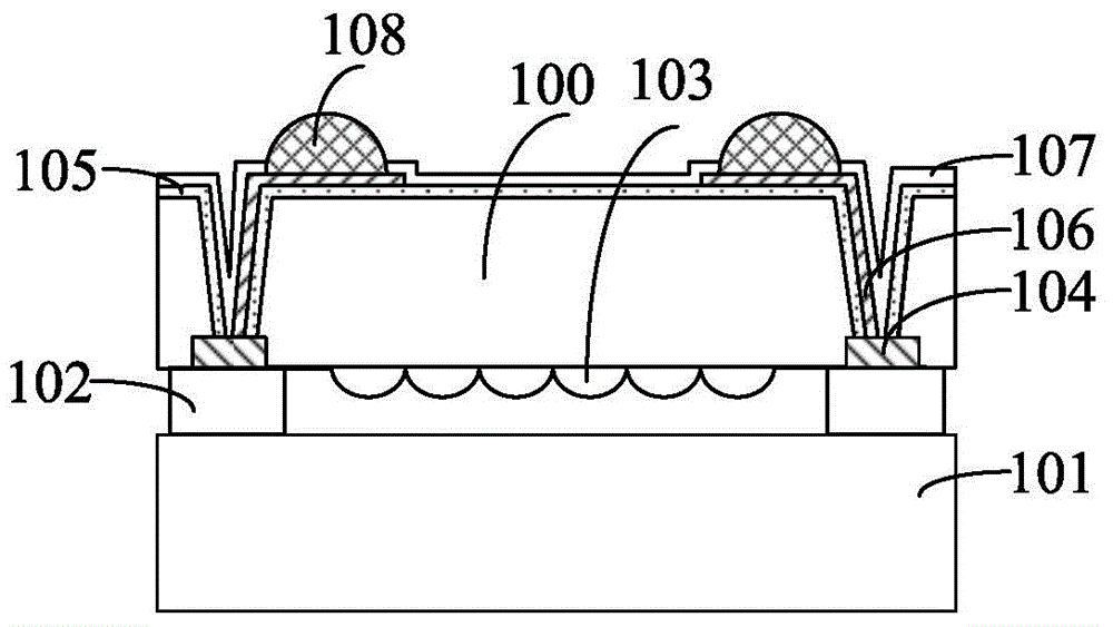
[0064] It can be seen from the background art that the packaging performance and reliability of the packaging structure provided by the prior art needs to be improved, and the process of forming the above packaging structure is relatively complicated, and the packaging cost is relatively high.

[0065] After research, it is found that the reasons why the packaging performance and reliability of the packaging structure need to be improved are:

[0066] First of all, the packaging process for forming the above-mentioned packaging structure is extremely complicated, and during the packaging process, the image sensor chip undergoes multiple packaging processes such as thinning, etching to form through holes, forming a protective layer, forming a metal layer, and forming an insulating layer. The above-mentioned packaging process has adverse effects on the performance of the image sensor chip, making it difficult for the performance of the formed packaging structure to reach an optim...


PUM


Abstract

The invention discloses a packaging method and packaging structures. The packaging method includes the steps of providing a plurality of individual image sensing chips, wherein each image sensing chip is provided with an image sensing area and a bonding pad surrounding the image sensing area; providing a PCB substrate, wherein a metal layer is formed on the surface of the PCB substrate; reversedly arranging the image sensing chips on the PCB substrate, wherein the bonding pads are electrically connected with the metal layer; forming a plastic sealing layer which covers the surface of the metal layer and the surfaces of the image sensing chips; forming a through hole, exposed out of the surface of the metal layer, in the plastic sealing layer; forming a welding protrusion which fully fills the through hole, wherein the top of the welding protrusion is higher than the surface of the plastic sealing layer; cutting the PCB substrate along the area of cutting lines to form the multiple single packaging structures. The packaging process is simple, the packaging structures have good packaging performance and high reliability, the packaging process can be partly conducted through the PCB manufacturing technology, and packaging process difficulty and packaging cost are reduced.

Description

technical field [0001] The invention relates to semiconductor packaging technology, in particular to a packaging method and a packaging structure. Background technique [0002] An image sensor is a sensor that senses external light and converts it into an electrical signal. After the image sensor chip is manufactured, a series of packaging processes are performed on the image sensor chip to form a packaged image sensor for use in various electronic devices such as digital cameras and digital video cameras. [0003] The traditional image sensor packaging method is usually packaged by wire bonding (Wire Bonding). However, with the rapid development of integrated circuits, longer leads make the product size unable to meet the ideal requirements. Therefore, wafer-level packaging (WLP: Wafer Level Package) has gradually replaced wire bonding packaging as a more commonly used packaging method. [0004] Such as figure 1 as shown, figure 1 It is a package structure, including: a...

Claims


Application Information

Patent Timeline
IPC IPC(8): H01L27/146
Inventor 王之奇喻琼王蔚
Owner CHINA WAFER LEVEL CSP
Why Eureka
Try Eureka