SOI NMOS ESD device and preparing method thereof

A device and acceptor technology, which is applied to SOI NMOS ESD devices and the field of preparing the SOI NMOS ESD devices, can solve the problems of SOINMOSESD devices being unsuitable, and achieve the effect of improving the effect of electrostatic discharge

Inactive Publication Date: 2014-08-20
SHANGHAI HUALI MICROELECTRONICS CORP
View PDF4 Cites 3 Cited by
  • Summary
  • Abstract
  • Description
  • Claims
  • Application Information

AI Technical Summary

Problems solved by technology

However, the above ESD acceptor doping ion implantation process is not suitable for SOI NMOS ESD devices
This is because the drain region of the SOI device is completely implanted with N+, and there is no space for ESD acceptor dopant ion implantation under the drain region, such as figure 2 Shown is a schematic structural diagram of an existing SOI NMOS device, wherein 00 represents the bottom silicon layer of the SOI substrate, 200 represents the intermediate dielectric layer of the

Method used


Image

  • SOI NMOS ESD device and preparing method thereof
  • SOI NMOS ESD device and preparing method thereof
  • SOI NMOS ESD device and preparing method thereof

Examples


Embodiment Construction

[0030] In order to make the content of the present invention clearer and easier to understand, the content of the present invention will be further described below in conjunction with the accompanying drawings. Of course, the present invention is not limited to this specific embodiment, and general replacements known to those skilled in the art are also covered within the protection scope of the present invention.

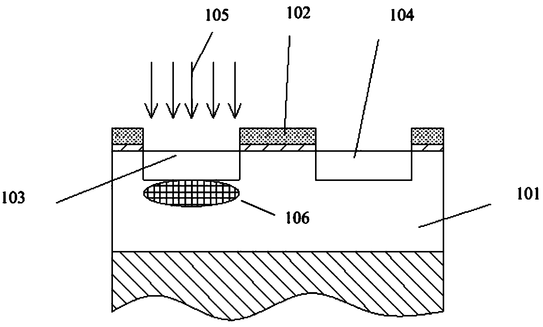
[0031] As mentioned above, in the SOI substrate, there is an intermediate dielectric layer under the bulk silicon region, so that there is no ion implantation space under the drain region, so the existing method of ESD ion implantation under the drain region is not suitable for SOI For the NMOS ESD device, the present invention improves the existing process by implanting acceptor dopant ions into the bottom of the channel, close to and contacting the side of the drain region, and away from the source and the surface of the bulk silicon region. In this way, The ESD ...


PUM


Abstract

The invention provides an SOI NMOS ESD device and a preparing method thereof. In a bulk silicon region, an ESD acceptor doping ion implantation region is formed on the bottom of a channel, being close to and making contact with the side edge of a drain region, and being far away from a source region and the surface of the bulk silicon region, and therefore the ESD acceptor doping ion implantation region can be applied to an SOI device; the ESD acceptor doping ion implantation region located at the position can guide ESD trigger currents to flow through the bulk silicon region, the depth range of the bulk silicon region is larger than that of the drain region, the effect of electrostatic discharge is improved, and breakdown voltage of the drain region is decreased.

Description

technical field [0001] The invention relates to the technical field of semiconductors, in particular to an SOI NMOS ESD device and a method for preparing the SOI NMOS ESD device. Background technique [0002] As semiconductor device technology continues to enter submicron and deep submicron, the reliability of electrostatic discharge protection (ESD) devices is becoming more and more important. In order to overcome the problem of decreased electrostatic discharge protection (ESD) capability brought about by the LDD structure, electrostatic discharge (ESD) ion implantation (ESD implant) technology is used to improve the electrostatic discharge (ESD) protection capability of NMOSESD devices, which is carried out under the drain The ESD acceptor dopant ion implantation reduces the breakdown voltage of the drain, which can improve the electrostatic protection capability of the NMOS ESD device. Usually, the ESD acceptor doping ion implantation uses boron for ion doping. Boron i...

Claims


Application Information

Patent Timeline
IPC IPC(8): H01L27/02H01L21/77H01L21/265H01L21/84
Inventor 颜丙勇
Owner SHANGHAI HUALI MICROELECTRONICS CORP
Why Eureka
Try Eureka