Transparent metal electrodes and their organic electroluminescent top-emitting devices
A transparent metal and luminescent technology, which is applied in the direction of electric solid-state devices, electrical components, semiconductor devices, etc., can solve the problems of poor performance of transparent top electrodes, achieve high uniformity of film formation, increase grain size, and increase electrical conductivity Effect
- Summary
- Abstract
- Description
- Claims
- Application Information
AI Technical Summary
Problems solved by technology
Method used
Image


Examples
Embodiment 1
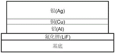
[0037] Embodiment 1: a kind of transparent metal electrode, such as figure 1 shown. The electrodes are arranged in the following order from bottom to top: substrate, interface layer, metal layer 1, metal layer 2, and metal layer 3, wherein:
[0038] The substrate is glass with better smoothness;
[0039] The interfacial layer is LiF deposited on glass with a thickness of 1 nm;
[0040] Metal layer 1 is Al deposited on the interface layer, with a thickness of 2 nm;
[0041] The metal layer 2 is Cu deposited on the metal layer 1 with a thickness of 1 nm;
[0042] The metal layer 3 is Ag deposited on the metal layer 2 with a thickness of 20 nm.
Embodiment 2
[0043] Embodiment 2: a kind of transparent metal electrode, such as figure 1 shown. The electrodes are arranged in the following order from bottom to top: substrate, interface layer, metal layer 1, and metal layer 2, wherein:
[0044] The substrate is glass with better smoothness;
[0045] The interfacial layer is LiF deposited on glass with a thickness of 1 nm;
[0046] Metal layer 1 is Al deposited on the interface layer, with a thickness of 2 nm;
[0047] Metal layer 2 is Ag deposited on metal layer 1 with a thickness of 20 nm.
[0048] Table 1 shows the electrode parameters in Example 1 and Example 2. By comparison, it is found that the Al / Cu / Ag three-layer metal electrode has smaller sheet resistance and surface roughness than the Al / Ag double-layer metal electrode.
[0049] In addition, through the comparison of the transmittance, it is found that compared with the Al / Ag double-layer metal electrode, the transmittance of the Al / Cu / Ag three-layer metal electrode has b...
Embodiment 3
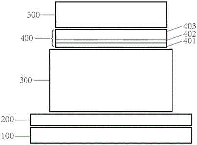
[0052] Embodiment 3: a kind of top emission organic electroluminescence device, such as Figure 4As shown, the layers of the device are arranged in the following order from bottom to top: substrate, bottom electrode, hole injection layer, hole transport layer, light emitting layer, electron transport layer, electron injection layer, top electrode and optical coupling output layer, wherein :
[0053] The substrate is coated with 500 nm SiO x Si slices;
[0054] The bottom electrode is Ag deposited on the substrate with a thickness of 100 nm;
[0055] The hole injection layer is MoO deposited on the bottom electrode 3 , with a thickness of 1.5 nm;
[0056] The hole transport layer is NPB deposited on the hole injection layer with a thickness of 60 nm;
[0057] The light-emitting layer is a doped layer Alq deposited on the hole transport layer 3 : C545T, the doping concentration is 1wt.%, and the thickness is 30nm;
[0058] The electron transport layer is Alq deposited on ...
PUM
| Property | Measurement | Unit |
|---|---|---|
| thickness | aaaaa | aaaaa |
| thickness | aaaaa | aaaaa |
| thickness | aaaaa | aaaaa |
Abstract
Description
Claims
Application Information
PatSnap Eureka turns technology decisions into work you can execute. Powered by our Innovation Knowledge Graph, it runs expert workflows across engineering, life sciences, materials and intellectual property. Get your review-ready output in minutes.


