Specimen preparation method for detecting subsurface damage depth of ultra-thin silicon wafer

A technology for subsurface damage and sample preparation, which is applied in the preparation of test samples, etc., can solve the problems of difficulty in obtaining the subsurface damage depth of ultra-thin silicon wafers, and achieve the effect of solving the problem of difficulty in obtaining and simple sample preparation method.

Active Publication Date: 2016-06-22
TIANJIN RES INST FOR ADVANCED EQUIP TSINGHUA UNIV
View PDF2 Cites 1 Cited by
  • Summary
  • Abstract
  • Description
  • Claims
  • Application Information

AI Technical Summary

Problems solved by technology

[0005] The invention proposes a sample preparation method for detecting the subsurface damage depth of an ultra-thin silicon wafer, which can effectively prepare an ultra-thin, fragile silicon wafer sample with a very thin damage layer, and the sample preparation method is simple and can Obtain clear subsurface microcracks, which solves the problem that the subsurface damage depth of ultra-thin silicon wafers is difficult to obtain

Method used


Image

  • Specimen preparation method for detecting subsurface damage depth of ultra-thin silicon wafer
  • Specimen preparation method for detecting subsurface damage depth of ultra-thin silicon wafer
  • Specimen preparation method for detecting subsurface damage depth of ultra-thin silicon wafer

Examples


Embodiment Construction

[0029] The present invention can be better understood from the following examples.

[0030] The silicon wafer used in this example has a diameter of 200 mm and a thickness of 200 μm; the steel plate used is cut by a hacksaw blade; the polishing liquid used is a diamond spray polishing liquid purchased from Naibo Testing Technology (Shanghai) Co., Ltd.; the polishing machine is a double-disk desktop metallographic Grinding and polishing machine; ultrasonic cleaner KQ3200DE CNC ultrasonic cleaner.

[0031] The steps are:

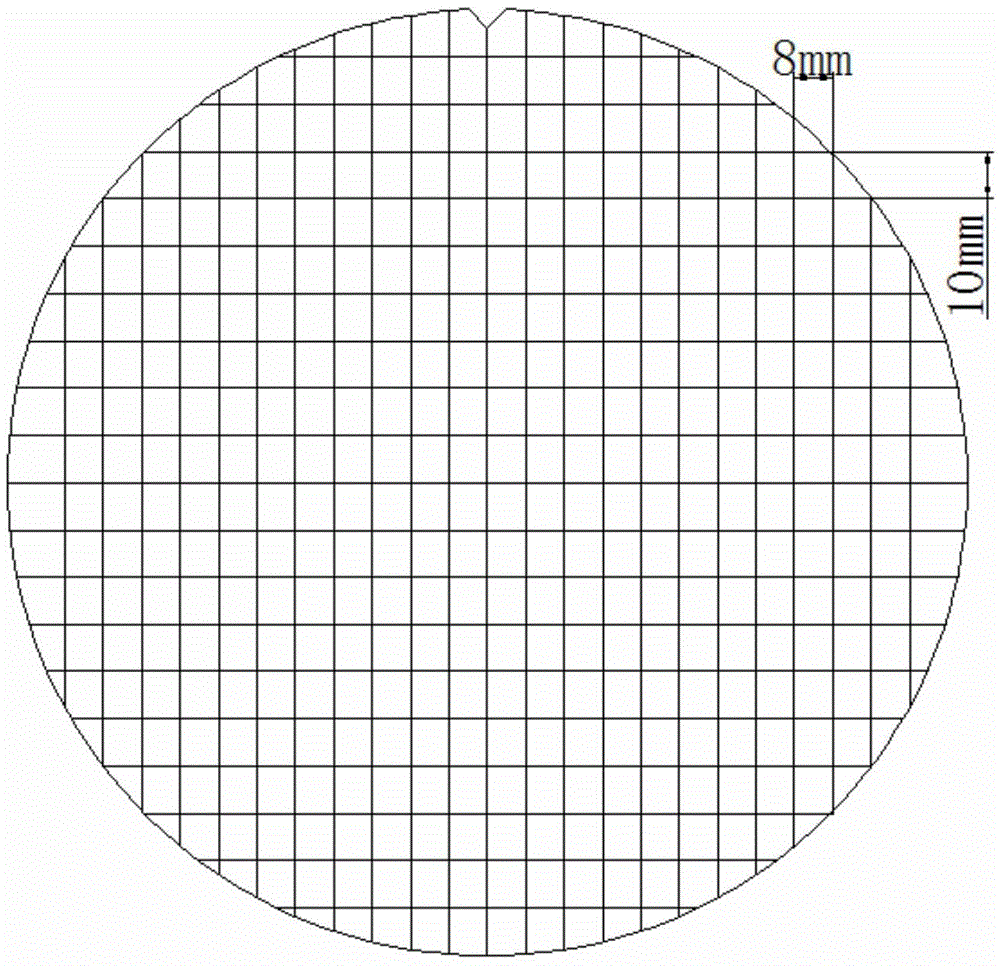
[0032] (1) Cut the entire wafer into multiple 10*8mm samples, such as figure 1 shown.

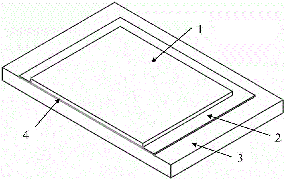
[0033] (2) Remove the sample at any position and paste it on the cut-off of the hacksaw blade. The edge of the wafer sample exceeds the edge of the steel plate, and the grinding surface of the wafer should be close to the position of the steel plate;

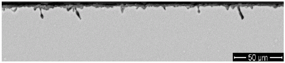
[0034] (3) Grind the pasted sample on a polishing machine with P800 sandpaper until the section to be observed is expos...


PUM

PropertyMeasurementUnit
thicknessaaaaaaaaaa
diameteraaaaaaaaaa
thicknessaaaaaaaaaa

Abstract

The invention discloses a sample preparation method for detecting the subsurface damage depth of an ultra-thin silicon wafer, which comprises the following steps: (1) cutting the entire wafer into multiple samples; (2) removing a sample at any position, and paste it on the metal plate; (3) grind, polish and corrode the pasted sample; the advantage of the present invention is that it can be used to prepare ultra-thin (thickness≤300μm), fragile silicon wafer The detection sample of the surface damage layer, and the sample preparation method is simple, can obtain clear subsurface microcracks, and solves the problem that the subsurface damage depth of the ultra-thin silicon wafer is difficult to obtain.

Description

technical field [0001] The invention relates to a detection technology for a silicon wafer damage layer, in particular to a method for preparing a silicon wafer subsurface damage detection sample. Background technique [0002] As the most important substrate material for integrated circuits, the quality of silicon wafers directly affects the performance and reliability of packaged devices. Graphics wafers require backside thinning to meet the thickness requirements for packaged chips. [0003] Grinding parameters (grain size, feed speed of grinding wheel, rotation speed of grinding wheel and rotary table) are different, and the degree of damage to the subsurface of the silicon wafer is different. Any small damage may cause the device to become a waste product. The subsurface damage depth is detected to evaluate the wafer processing quality and provide guidance for silicon wafer thinning parameters. [0004] Destructive detection methods are often used to detect the depth o...

Claims


Application Information

Patent Timeline
Patent Type & Authority Patents(China)
IPC IPC(8): G01N1/32
Inventor 秦飞闫德宝孙敬龙安彤王仲康唐亮
Owner TIANJIN RES INST FOR ADVANCED EQUIP TSINGHUA UNIV
Why Eureka
Try Eureka