Low Dropout Linear Regulators

A low-dropout linear and voltage regulator technology, which is applied in the direction of instruments, electrical variable adjustment, control/regulation systems, etc., can solve the problems of high overall power consumption and high circuit power consumption, and achieve low noise, high PSRR, and low power consumption Effect

Active Publication Date: 2015-12-09
NANJING CHIPOWER ELECTRONICS
View PDF6 Cites 0 Cited by
  • Summary
  • Abstract
  • Description
  • Claims
  • Application Information

AI Technical Summary

Problems solved by technology

[0004] The above-mentioned circuit structure can achieve a higher-precision regulated output, but since the entire circuit structure includes the bandgap reference source BGR and the operational amplifier AMP, the overall power consumption of the circuit is relatively high. If you want to pursue higher PSRR and faster response speed and lower output noise, the power consumption of the circuit will be higher

Method used


Image

  • Low Dropout Linear Regulators
  • Low Dropout Linear Regulators
  • Low Dropout Linear Regulators

Examples


specific Embodiment 1

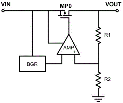
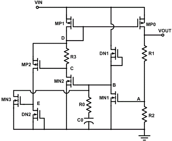
[0021] Such as figure 2 The low-dropout linear regulator shown includes: an enhanced PMOS transistor MP0 (output MOS transistor), and a voltage sampling circuit connected in series to the current outflow terminal of the output MOS transistor (that is, the drain of the enhanced PMOS transistor MP0). The sampling signal and the reference voltage value obtain the voltage comparison circuit of the error signal, and the Buffer driving circuit that outputs the MOS tube is driven by the error signal. The voltage sampling circuit is composed of resistors R1 and R2 connected in series, and the connection point A of the resistors R1 and R2 outputs a sampling signal VA.

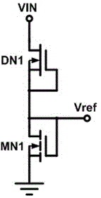
[0022] The voltage comparison circuit includes: depletion-type NMOS tube DN1, enhanced NMOS tube MN1, the drain of the depletion-type NMOS tube DN1 is connected to the input power supply VIN, the gate and source of the depletion-type NMOS tube DN1 are short-circuited and then connected to the enhanced NMOS The drain o...

specific Embodiment 2

[0026] On the basis of Embodiment 1, further optimize the design of the Buffer drive circuit. The Buffer drive circuit includes: enhanced PMOS transistor MP1, resistor R3, enhanced NMOS transistor MN2, the source of the enhanced PMOS transistor MP1 is connected to the input power supply, the gate and drain of the enhanced PMOS transistor MP1 are short-circuited and then connected to one end of the resistor R3 (point D), the other end of the resistor R3 is connected to the drain of the enhanced NMOS transistor MN2 (point C), the gate of the enhanced NMOS transistor MN2 is connected to the drain of the enhanced NMOS transistor MN1, and the source of the enhanced NMOS transistor MN2 is grounded.

[0027] figure 2 In the circuit shown, the gate of the enhanced NMOS transistor MN1 is separated from the drain, the gate of the enhanced NMOS transistor MN1 is connected between the resistor R1 and the resistor R2 as the input terminal of the voltage comparison circuit, and the enhance...

specific Embodiment 3

[0029] In order to limit the excessive output current of the enhanced PMOS transistor MP0, the present invention designs a current limiting protection circuit by utilizing the feature that the enhanced PMOS transistor MP1 in the Buffer drive circuit can copy the current of the enhanced PMOS transistor MP0. The current limiting protection circuit includes: enhanced PMOS transistor MP2, enhanced NMOS transistor MN3, depleted NMOS transistor DN2, the source of the enhanced PMOS transistor MP2 is connected to the drain of the enhanced PMOS transistor MP1, and the gate of the enhanced PMOS transistor MP2 is connected to the enhanced The drain of the enhanced NMOS transistor MN2, the drain of the enhanced PMOS transistor MP2 is connected to the drain of the depleted NMOS transistor DN2 (point E), the gate and source of the depleted NMOS transistor DN2 are shorted and grounded, and the drain of the enhanced NMOS transistor MN3 The pole is connected to the drain of the enhanced NMOS tr...


PUM


Abstract

The invention discloses a low-dropout linear voltage stabilizer, and belongs to the technical field of integrated circuits. The low-dropout linear voltage stabilizer comprises an output MOS tube, a voltage sampling circuit connected to the current outflow end of the output MOS tube in series, a voltage comparison circuit comparing a sampled signal with a standard voltage value to obtain an error signal, and a Buffer drive circuit driving the output MOS tube to work through the error signal. The voltage comparison circuit comprises a first depletion type NMOS tube and a first enhancement type NMOS tube. The voltage comparison function is achieved through a standard voltage generation circuit, and the domain area is reduced. The low drop-out linear voltage stabilizer has the advantages of being low in power consumption, low in noise and high in PSRR.

Description

technical field [0001] The invention discloses a low-dropout linear regulator, in particular a low-power, low-noise LDO (Low Dropout Regulator, low-dropout linear regulator), which belongs to the technical field of integrated circuits. Background technique [0002] Regardless of whether portable electronic devices are powered by AC adapters or batteries, the power supply voltage will vary in a wide range during operation. In order to ensure the stability of the power supply voltage, almost all electronic devices are powered by voltage regulators. Small precision electronic equipment also requires a very clean power supply (no ripple, no noise), so as not to affect the normal operation of electronic equipment. Therefore, LDO circuits generally need to meet the requirements of wide operating voltage range, regulated output, low noise, high PSRR, high transient response speed, and low static power consumption. At present, most LDO circuits adopt the structure of a bandgap refe...

Claims


Application Information

Patent Timeline
Patent Type & Authority Patents(China)
IPC IPC(8): G05F1/56
Inventor 黄九洲夏炎
Owner NANJING CHIPOWER ELECTRONICS
Why Eureka
Try Eureka