Shift register unit, gate drive circuit and display device

A shift register and gate technology, applied in static memory, digital memory information, instruments, etc., can solve the problem that the shift register unit cannot realize bidirectional scanning, the time for the fourth transistor to apply a high level is short, and the brightness of the display device is not high. Equalize problems to achieve the effect of increasing achievability, reducing erroneous output, and simplifying structure

Active Publication Date: 2014-10-01
HEFEI BOE OPTOELECTRONICS TECH +1
View PDF5 Cites 48 Cited by
  • Summary
  • Abstract
  • Description
  • Claims
  • Application Information

AI Technical Summary

Problems solved by technology

[0010] The disadvantage of this shift register unit is that the fourth transistor M4 applies a high level for a very short time, and will not drift under the DC bias voltage. Most of the time, PU and OUTPUT are in a floating state, which is easy for other parasitic Capacitance, etc., resulting in misoperation
This will lead to uneven brightness of the display device and affect the quality of the product
At the same time, this kind of shift register unit cannot realize bidirectional scanning, and the clock signal CLK will generate coupling (Coupling) noise voltage

Method used


Image

  • Shift register unit, gate drive circuit and display device
  • Shift register unit, gate drive circuit and display device
  • Shift register unit, gate drive circuit and display device

Examples


no. 1 example

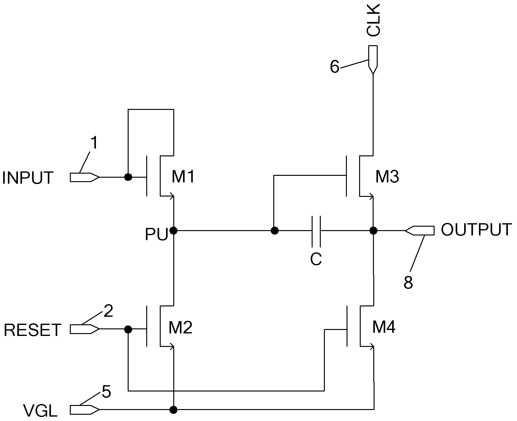
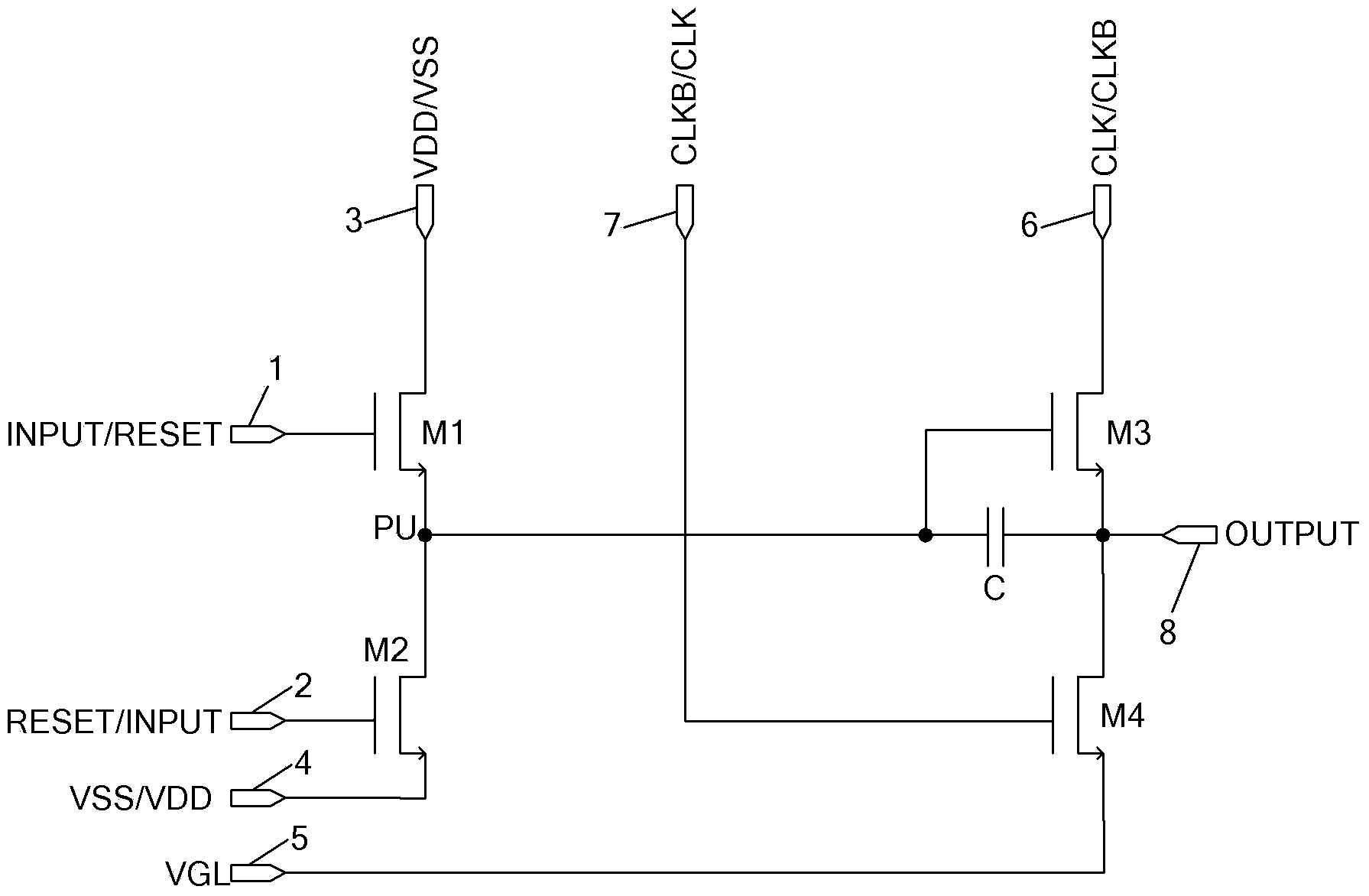
[0044] The first embodiment is a basic implementation circuit of the shift register unit of the present invention, and a basic cascaded circuit constituting the gate drive circuit. figure 2 is a circuit diagram of the shift register unit of this first embodiment. Such as figure 2 As shown, the shift register unit of this embodiment includes at least seven input terminals and one output terminal, and at least four transistors and one capacitor.

[0045] The seven input terminals are the first input terminal 1 , the second input terminal 2 , the third input terminal 3 , the fourth input terminal 4 , the constant low level terminal 5 , the first clock terminal 6 and the second clock terminal 7 . One output is the output 8 . The four transistors are first to fourth transistors M1 to M4. One capacitor is capacitor C.

[0046] The gate of the first transistor M1 is connected to the first input terminal 1, and the source is connected to the third input terminal 3; the gate of t...

no. 2 example

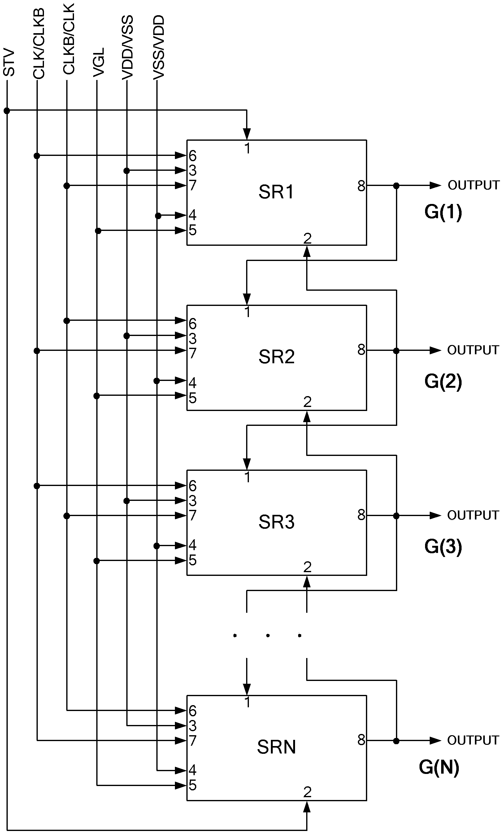
[0069] The second embodiment is an improvement on the basis of the first embodiment. The cascading manner of the gate driving circuits of this embodiment is the same as that of the first embodiment, the difference is the structure of each shift register unit. Figure 5 The circuit configuration of the shift register unit of this embodiment is shown. Such as Figure 5 As shown, compared with the first embodiment, the shift register unit of this embodiment further includes a fifth transistor M5. The source and gate of the fifth transistor M5 are connected, and the source is connected to the second clock terminal 7 , and the drain is connected to the gate of the fourth transistor M4 .

[0070] The function of the fifth transistor M5 is: after the reset period, when the clock signal connected to the second clock terminal 7 is at a low level, the gate of the fourth transistor M4 and the second clock terminal 7 are not conducted to maintain relatively low voltage. High potential,...

no. 3 example

[0072] The third embodiment is also an improvement on the mobile register unit based on the first embodiment. Likewise, the cascading manner of the gate drive circuits of this embodiment is the same as that of the first embodiment, except for the structure of each shift register unit. Image 6 The circuit configuration of the shift register unit of the third embodiment is shown. Such as Image 6 As shown, compared with the first embodiment, the shift register unit of the third embodiment may further include a sixth transistor M6, the source of the sixth transistor M6 is connected to the gate of the fourth transistor M4, and the sixth transistor M6 The drain of M6 is connected to the constant low level terminal 5 . Here, the connection node of the gate of the fourth transistor M4 is referred to as a pull-down node PD.

[0073] In this way, during the pre-charging period and the scan period of the current stage, when the pull-up node PU is at a high voltage, the sixth transis...


PUM


Abstract

The invention discloses a bidirectional scanning gate drive circuit and a shift register unit of the bidirectional scanning gate drive circuit. The shift register unit comprises a first input end (1), a second input end (2), a first clock end (6) and an output end (8). A shift trigger signal and a reset signal are connected into the first input end (1) and the second input end (2) respectively. When forward shift and backward shift are switched, the signals connected into the first input end (1) and the second input end (2) are switched; a clock signal is connected into the first clock end (6), and the clock signal is used for providing drive level for the output end (8). The circuit of the shift register unit can be composed of at least four transistors and one capacitor. The circuit of the shift register unit is simple in structure, and the problem of coupled noise voltage caused by the clock signal can be solved.

Description

technical field [0001] The invention belongs to the technical field of circuit driving, and in particular relates to a shift register unit, a gate drive circuit (gate drive IC) and a display device using the shift register unit. Background technique [0002] The driving circuit of the display device mainly includes a gate driving circuit (scanning driving circuit) and a data driving circuit (or source driving circuit), wherein the gate driving circuit includes cascaded shift register units, and the input clock signal CLK is shifted After the conversion of the register unit, it will be sequentially added to the gate line of each pixel row of the display device, so as to control the display of the display device row by row. [0003] The circuit of the existing shift register unit such as figure 1 As shown, it includes four transistors and two capacitors, that is, a first transistor M1, a second transistor M2, a third transistor M3, a fourth transistor M4, and a capacitor C. ...

Claims


Application Information

Patent Timeline
Patent Type & Authority Applications(China)
IPC IPC(8): G09G3/36G11C19/28
CPCG11C19/287G09G3/20G09G2310/0267G09G2310/0286
Inventor 邵贤杰李小和古宏刚
Owner HEFEI BOE OPTOELECTRONICS TECH
Why Eureka
Try Eureka