Supercharge Your Innovation With Domain-Expert AI Agents!

Inductance structure and method for making same

A manufacturing method and inductance technology, applied in the direction of inductors, circuits, electrical components, etc., can solve the problem that the performance of planar inductance needs to be further improved, and achieve the effect of reducing eddy current, improving performance, and improving Q value.

Active Publication Date: 2014-10-08
SHANGHAI HUAHONG GRACE SEMICON MFG CORP
View PDF6 Cites 2 Cited by
  • Summary
  • Abstract
  • Description
  • Claims
  • Application Information

AI Technical Summary

Problems solved by technology

Therefore, the performance of the planar inductor needs to be further improved.

Method used


Image

  • Inductance structure and method for making same
  • Inductance structure and method for making same
  • Inductance structure and method for making same

Examples


Embodiment Construction

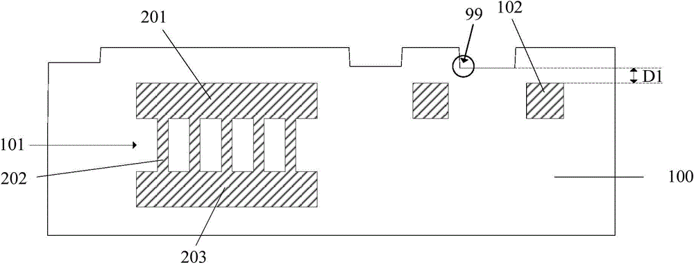
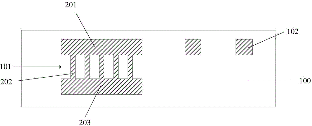
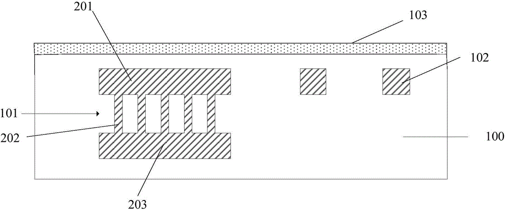
[0034] In the prior art, the inductance value of the inductance can be increased by arranging magnetic materials inside the inductance coil. However, the method of arranging magnetic materials inside the inductance coil to increase the inductance value of the inductance may generate magnetic The residue of the material and the residue of the magnetic material are in the shape of a ring, which may generate a large eddy current when the inductance coil is working, which increases the energy loss of the inductance coil and reduces the Q value of the inductance. The Q value of the inductance is also called the quality factor of the inductance, which is the main parameter to measure the inductance device. It refers to the ratio of the inductive reactance presented by an inductor to its equivalent loss resistance when it operates under an AC voltage of a certain frequency. The higher the Q value of the inductor, the smaller the loss and the higher the efficiency.

[0035] In order ...


PUM


Abstract

The invention provides an inductance structure and a method for making the same. The method for making the inductance structure comprises the following steps that a substrate is provided; a dielectric layer and an inductance coil are formed on the substrate, wherein the inductance coil is located in the dielectric layer, and the inductance coil is covered with the dielectric layer; the surface of the dielectric layer is flattened; a first groove is formed in the region, located in the inductance coil, of the dielectric layer; a magnetic layer is formed in the first groove. The inductance structure comprises the dielectric layer, the inductance coil and the magnetic layer, wherein the upper surface of the dielectric layer is flat, the inductance coil is located in the dielectric layer, and the magnetic layer is located in the region, located in the inductance coil, of the dielectric layer. The magnetic layer can increase the inductance value of the inductance coil. Because the surface of the dielectric layer is flattened, the upper surface of the dielectric layer can be kept flat, and the situation that a step is generated due to influence of the inductance coil is avoided. No annular residue is formed on the step after the magnetic layer on the dielectric layer is removed, and therefore an eddy current can be reduced, the Q value of the inductance coil can be increased, and the performance of the inductance coil can be improved.

Description

technical field [0001] The invention relates to the field of semiconductors, in particular to a method for manufacturing an inductance structure and the inductance structure. Background technique [0002] In an existing integrated circuit (such as a CMOS radio frequency integrated circuit), an inductor is an important electrical device, and its performance parameters directly affect the performance of the integrated circuit. In the prior art, planar inductors are mostly used as inductors in integrated circuits, such as planar spiral inductors. The planar inductor is a planar inductor coil structure, and the planar inductor coil is formed by winding metal wires on the surface of the substrate or dielectric layer. Compared with the traditional wire wound inductor, the planar inductor has the advantages of low cost, easy integration, low noise and low power consumption. The advantage of being low, more importantly, it is compatible with today's integrated circuit technology. ...

Claims


Application Information

Patent Timeline
Patent Type & Authority Applications(China)
IPC IPC(8): H01L21/768H01L23/522
CPCH01L28/10
Inventor 黎坡
Owner SHANGHAI HUAHONG GRACE SEMICON MFG CORP
Features
  • R&D
  • Intellectual Property
  • Life Sciences
  • Materials
  • Tech Scout
  • Unparalleled Data Quality
  • Higher Quality Content
  • 60% Fewer Hallucinations
Learn More