Semiconductor device with MIM capacitor and formation method thereof

A semiconductor and capacitor technology, applied in the field of semiconductor devices with MIM capacitors and their formation, can solve problems to be improved, and achieve the effect of reducing resistance and improving performance

Inactive Publication Date: 2014-10-15
SEMICON MFG INT (SHANGHAI) CORP
View PDF5 Cites 7 Cited by
  • Summary
  • Abstract
  • Description
  • Claims
  • Application Information

AI Technical Summary

Problems solved by technology

[0004] However, the performance of semiconductor devices with MIM capacitors formed in the prior art still needs to be improved. How to further improve the performance of semiconductor devices with MIM capacitors is an urgent problem to be solved at present

Method used


Image

  • Semiconductor device with MIM capacitor and formation method thereof
  • Semiconductor device with MIM capacitor and formation method thereof
  • Semiconductor device with MIM capacitor and formation method thereof

Examples


no. 1 example

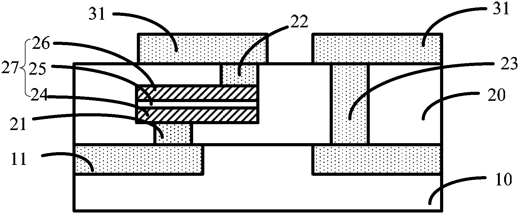
[0043] Specifically, please refer to Figure 2-Figure 9 , Figure 2-Figure 9 A schematic cross-sectional structure showing the formation process of the semiconductor device with MIM capacitor according to the first embodiment of the present invention.

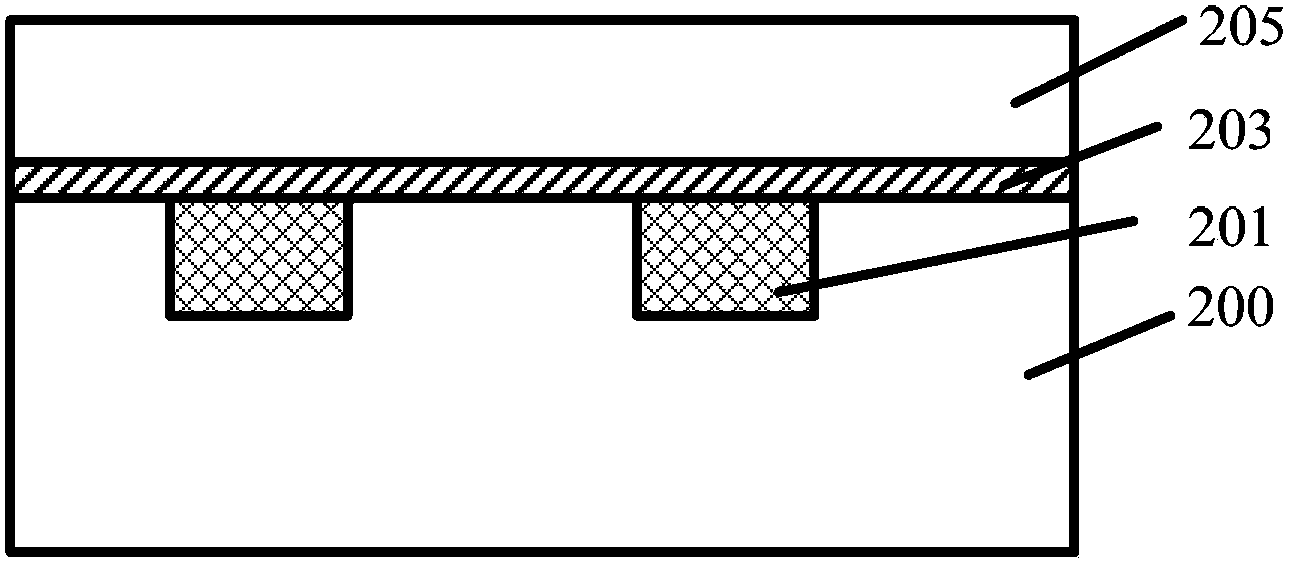
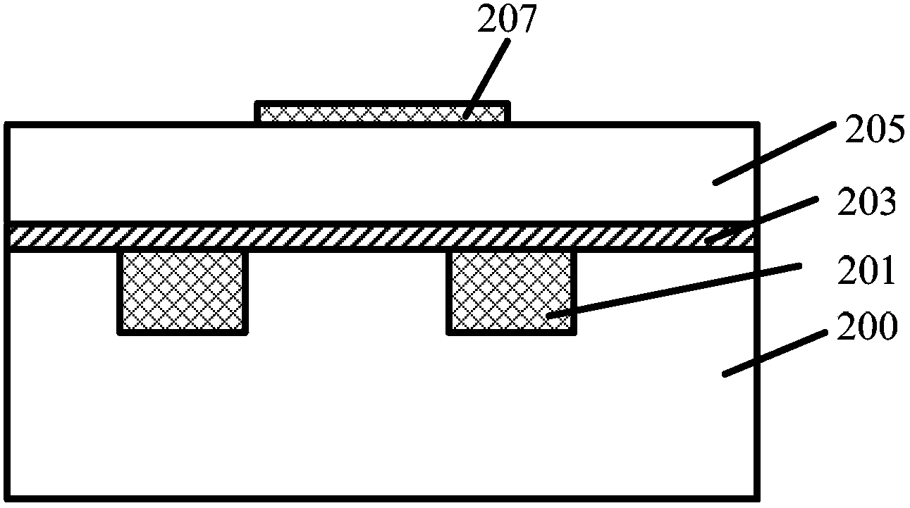
[0044] Please refer to figure 2 , providing a substrate 200 and a first interlayer dielectric layer 205 covering the substrate 200 .

[0045] The base 200 is used to provide a platform for subsequent processes, and the base 200 includes a semiconductor substrate (not shown) and an initial interlayer dielectric layer (not shown) on the surface of the semiconductor substrate. Wherein, the material of the semiconductor substrate is single crystal silicon, single crystal germanium, III-V compound or silicon-on-insulator, etc., and the material of the initial interlayer dielectric layer is low-K material, ultra-low-K material or oxide Wait.

[0046] In the embodiment of the present invention, it also includes: forming an intercon...

no. 2 example

[0097] Different from the first embodiment of the present invention, only one conductive plug is electrically connected to the interconnection metal layer 301 in the second embodiment.

[0098] Please refer to Figure 10 , Figure 10 A schematic cross-sectional structure showing the formation process of the semiconductor device with MIM capacitor according to the second embodiment of the present invention.

[0099] providing a substrate 300 and a first interlayer dielectric layer 305 covering the substrate 300;

[0100] forming an interconnect metal layer 301 within the substrate;

[0101] forming a MIM capacitor located on the surface of the first interlayer dielectric layer 305, the MIM capacitor comprising a bottom electrode layer 307 and a top electrode layer 311a which are isolated from each other and crossed laterally;

[0102] forming a second interlayer dielectric layer 315 covering the surface of the MIM capacitor and the first interlayer dielectric layer 305;

[...


PUM


Abstract

Provided is a semiconductor device with an MIM capacitor and a formation method thereof. The formation method comprises the steps that a substrate and a first layer-to-layer dielectric layer which covers the substrate are provided; the MIM capacitor which is arranged on the surface of the first layer-to-layer dielectric layer is formed, wherein the MIM capacitor comprises a bottom part electrode layer and a top part electrode layer which are mutually isolated and transversely staggered; a second layer-to-layer dielectric layer which covers the MIM capacitor and the surface of the first layer-to-layer dielectric layer is formed; and a first conductive plug and a second conductive plug which penetrate trough the second layer-to-layer dielectric layer are formed. The first conductive plug is contacted with the side wall and the partial surface of the top part electrode layer of the MIM capacitor. The second conductive plug is contacted with the side wall and the partial surface of the bottom part electrode layer of the MIM capacitor. The formed semiconductor device is low in resistance and excellent in performance.

Description

technical field [0001] The invention relates to the technical field of semiconductors, in particular to a semiconductor device with an MIM capacitor and a forming method thereof. Background technique [0002] Capacitive components are often used as electronic passive devices in integrated circuits such as radio frequency ICs and monolithic microwave ICs. Common capacitors include metal oxide semiconductor (MOS) capacitors, PN junction capacitors, and MIM (metal-insulator-metal, MIM for short) capacitors. Among them, MIM capacitors have the least interference on transistors and can provide better linearity (Linearity) and symmetry (Symmetry). Therefore, they have been widely used, especially in mixed-signal (Mixed-signal) and radio frequency ( RF, Radio Frequency) field. [0003] Please refer to figure 1 , the semiconductor device with MIM capacitor in the prior art comprises: a dielectric layer 10, a first metal layer 11 positioned on the surface of the dielectric layer 1...

Claims


Application Information

Patent Timeline
Patent Type & Authority Applications(China)
IPC IPC(8): H01L21/02H01L23/522
CPCH01L28/40H01L23/5223H01L2924/0002H01L21/76897H01L2924/00
Inventor 洪中山
Owner SEMICON MFG INT (SHANGHAI) CORP
Why Eureka
Try Eureka