Wave aberration measuring device

A measuring device and a technology for wave aberration, which are applied in photoplate-making process exposure devices, optical performance testing, microlithography exposure equipment, etc. Signal strength, enhanced compactness, reduced requirements

Active Publication Date: 2014-10-22
SHANGHAI MICRO ELECTRONICS EQUIP (GRP) CO LTD
View PDF6 Cites 6 Cited by
  • Summary
  • Abstract
  • Description
  • Claims
  • Application Information

AI Technical Summary

Problems solved by technology

[0005] The disadvantages of this solution are: 1. The 0th-order diffracted light diffracted by the grating will have a stronger light intensity, so that the positive and negative 1st-order diffracted light used for measurement will have a weaker light intensity; 2. Because the 0th-order light is not used in the measurement, Therefore, it is necessary to filter out the 0th-order light, and it is easy to generate stray light when filtering out the 0-order diffracted light; 3. The separation design of the grating and the order mask causes the structure to be complicated

Method used


Image

  • Wave aberration measuring device
  • Wave aberration measuring device
  • Wave aberration measuring device

Examples


Embodiment 1

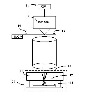
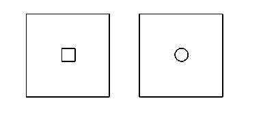
[0027] Such as figure 2 As shown, the wave aberration measurement device of the present invention includes two parts: an object plane mask 13 and an image plane detection unit 19 . On the object plane mask 13, small hole marks are included, and the small hole marks can be circular or square, such as image 3 As shown, the size of the small hole mark can be taken as 700nm. The image plane detection unit 19 includes a substrate 15 and a detector 18 . The upper surface of the substrate 15 includes grating marks 16, the line width of the grating marks is 600nm, and the period is 1200nm. The substrate can be made of fused silica glass, and the thickness of the substrate can be 6.35 mm. The lower surface of the base 15 contains the window marked 1.5 mm. The lower surface of the substrate 15 coincides with the best focus plane of the projection objective. The structure of the grating mark 16 is as Figure 4 As shown, there are marks in two directions, and the two marks are per...

Embodiment 2

[0035] In another embodiment of the present invention, the structure of the grating mark 16 on the substrate 15 is as Figure 6 As shown, it is a two-dimensional grating. Each marking period includes two light-transmitting regions and two light-transmitting regions, wherein the marking line widths of the light-transmitting region and the light-impermeable region are equal. During the marking period, the difference in optical path between the light beams passing through the light-transmitting area 1 and the light-transmitting area 2 is 180 degrees.

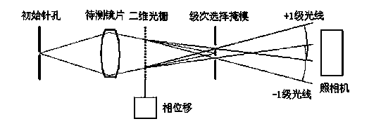
[0036] During measurement, the light emitted by the light source 11 is incident on the object plane mask 13 on the mask table 14 after passing through the illumination system 12, and the small holes of the object plane mask 13 diffract the beam to form an ideal spherical wave. After passing through the projection objective lens, a spherical wave carrying the wave aberration of the projection objective lens is formed. The spherica...


PUM


Abstract

This invention provides a wave aberration measuring device used for measuring the wave aberration of a projection objective of a photo-etching device. The wave aberration measuring device comprises a light source, a lightning system, an object plane mask, a projection objective, and an image plane detection unit. Light emitted by the light source passes through the lighting system to form a lighting beam, and the lighting beam is incident on the object plane mask on an object plane of the projection objective. The object plane mask includes a small hole tag, and the lighting beam is diffracted through a small hole to form an ideal spherical wave. The ideal spherical wave passes through the projection objective to form a spherical wave carrying wave aberration of the projection objective, and the spherical wave is projected on the image plane detection unit. The image plane detection unit detects the spherical wave carrying wave aberration of the projection objective to acquire wave aberration information of the projection objective. The wave aberration measuring device is characterized in that the image plane detection unit includes a base and a detector, the upper surface of the base contains a grating tag, the lower surface of the base contains a window tag, the spherical wave carrying wave aberration of the projection objective is diffracted through the grating tag to generate light at a +1 level and light at a -1 level, the light at a +1 level and the light at a -1 level converge at the window tag on the lower surface of the base, the light at a +1 level and the light at a -1 level overlap and interfere with each other to form an interference image after passing through the window tag, and the interference image is recorded by the detector.

Description

technical field [0001] The invention relates to the technical field of semiconductor manufacturing, in particular to a wave aberration measuring device used for a projection objective lens of a lithographic equipment. Background technique [0002] One goal of the semiconductor industry is to integrate more electronic components into a single integrated circuit (IC). To achieve this goal, the size of the components must be continuously reduced, that is, the resolution of the lithography projection system must be continuously improved. Objective lens wave aberration is an important factor limiting the resolution of a projection system, and it is an important cause of line width variation. [0003] Although the objective lens has been strictly inspected and optimized during the manufacturing and assembly process to minimize its wave aberration, it is still necessary to perform online wave aberration measurement after the objective lens system is integrated into the lithography...

Claims


Application Information

Patent Timeline
Patent Type & Authority Applications(China)
IPC IPC(8): G01M11/02G03F7/20
Inventor 马明英
Owner SHANGHAI MICRO ELECTRONICS EQUIP (GRP) CO LTD
Why Eureka
Try Eureka