Semiconductor structure and forming method thereof

A technology of semiconductor and gate structure, applied in the field of semiconductor structure and its formation, can solve the problems of semiconductor device performance obstruction, reduce carrier mobility in the channel region of PMOS transistor, etc., and achieve reduced tensile stress, good performance, and increased effect of distance

Active Publication Date: 2014-10-29
SEMICON MFG INT (SHANGHAI) CORP
View PDF5 Cites 32 Cited by
  • Summary
  • Abstract
  • Description
  • Claims
  • Application Information

AI Technical Summary

Problems solved by technology

[0006] However, although the tensile stress can improve the performance of the NMOS transistor, the first conductive layer 104 will also provide the tensile stress to the first fin portion 102, correspondingly reducing the carrier mobility in the channel region of the PMOS transistor, which is still very important for improving the performance of the semiconductor transistor. Device performance hindered

Method used


Image

  • Semiconductor structure and forming method thereof
  • Semiconductor structure and forming method thereof
  • Semiconductor structure and forming method thereof

Examples


Embodiment Construction

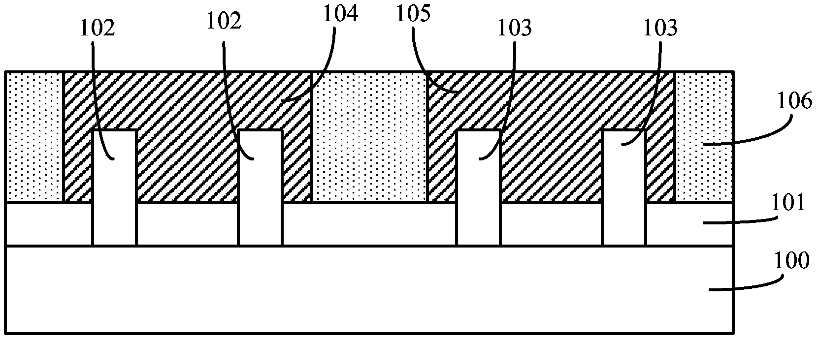
[0033] As mentioned in the background, the tensile stress provided by the conductive layer to the PMOS fin field effect transistor will reduce the mobility of carriers in its channel region and reduce the performance of the semiconductor device.

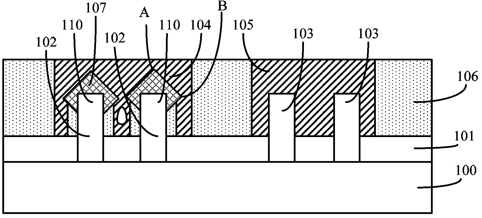
[0034] After research by the inventors of the present invention, a PMOS fin field effect transistor with raised source and drain regions (raised source / drain) is proposed. Such as figure 2 Shown is a schematic diagram of the cross-sectional structure of a fin field effect transistor with raised source and drain regions. figure 1On the basis of the above, it also includes: the source region and the drain region 110 located in the first fin portion 102; the semiconductor layer 107 located on the top and part of the sidewall surface of the source region and the drain region 110 of the first fin portion 102, the semiconductor layer The portion 107 located on the top surface of the first fin portion 102 has a raised corner A, and the fi...


PUM


Abstract

Provided are a semiconductor structure and a forming method thereof. The forming method comprises the steps that a semiconductor layer is formed in a source region and a drain region of a first fin part, covers the top surface and part of the side wall surface of the first fin part and is provided with protruded first ridge corners and second ridge corners, the first ridge corners are located on the top surface of the first pin part, and the second ridge corners are located on the surface of a side wall of the first fin part; a barrier layer is formed on a substrate, the first fin part and the surface of the semiconductor layer and fills a space between the adjacent second ridge corners, so that the adjacent second ridge corners are connected through the barrier layer; a dielectric layer is formed on the surface of the barrier layer, a first opening in the dielectric layer is exposed out of the barrier layer on the surfaces of at least two adjacent first ridge corners, the position of a side wall of the first opening in contact with the barrier layer is higher than the horizontal positions of the second ridge corners; the barrier layer at the bottom of the first opening is etched until the barrier layer is exposed out of the surface of the semiconductor layer, and a first conductive layer is formed on the surface of the semiconductor layer in the first opening. The performance of a formed semiconductor device is improved.

Description

technical field [0001] The invention relates to the technical field of semiconductor manufacturing, in particular to a semiconductor structure and a forming method thereof. Background technique [0002] With the rapid development of semiconductor manufacturing technology, semiconductor devices are developing towards higher element density and higher integration. As the most basic semiconductor device, transistors are currently being widely used. Therefore, with the increase of component density and integration of semiconductor devices, the gate size of planar transistors is getting shorter and shorter. The ability of traditional planar transistors to control channel current Weakened, resulting in short channel effect, resulting in leakage current, and ultimately affecting the electrical performance of semiconductor devices. [0003] In order to overcome the short channel effect of the transistor and suppress the leakage current, the prior art proposes a Fin Field Effect Tra...

Claims


Application Information

Patent Timeline
Patent Type & Authority Applications(China)
IPC IPC(8): H01L21/336H01L21/8238H01L29/78H01L29/06H01L27/092
CPCH01L21/823807H01L27/092H01L29/0642H01L29/66795H01L29/785
Inventor 洪中山
Owner SEMICON MFG INT (SHANGHAI) CORP
Why Eureka
Try Eureka