Low-electric-leakage and low-forward-voltage-drop Schottky diode structure and manufacturing method of low-electric-leakage and low-forward-voltage-drop Schottky diode structure

A diode and Schottky potential technology, applied in the field of diodes and their preparation, can solve the problems of increased forward voltage drop, increased leakage current, etc., to reduce forward voltage drop, reduce reverse leakage current, and preparation method simple effect

Inactive Publication Date: 2014-11-05
SHANGHAI ANWEI ELECTRONICS
View PDF5 Cites 8 Cited by
  • Summary
  • Abstract
  • Description
  • Claims
  • Application Information

AI Technical Summary

Problems solved by technology

In the manufacturing process, the oxide layer is generally grown by thermal oxidation, and the oxide layer has the characteristics of boron absorption and phosphorus removal. For N-type materials, the concentration of the surface layer increases, such as figure 2 As shown, the barrier height will be reduced and the leakage current will increase. Therefore, epitaxial wafers or high barrier metals with high resistivity should be selected, which will lead to an increase in forward voltage drop.

Method used


Image

  • Low-electric-leakage and low-forward-voltage-drop Schottky diode structure and manufacturing method of low-electric-leakage and low-forward-voltage-drop Schottky diode structure
  • Low-electric-leakage and low-forward-voltage-drop Schottky diode structure and manufacturing method of low-electric-leakage and low-forward-voltage-drop Schottky diode structure
  • Low-electric-leakage and low-forward-voltage-drop Schottky diode structure and manufacturing method of low-electric-leakage and low-forward-voltage-drop Schottky diode structure

Examples


Embodiment

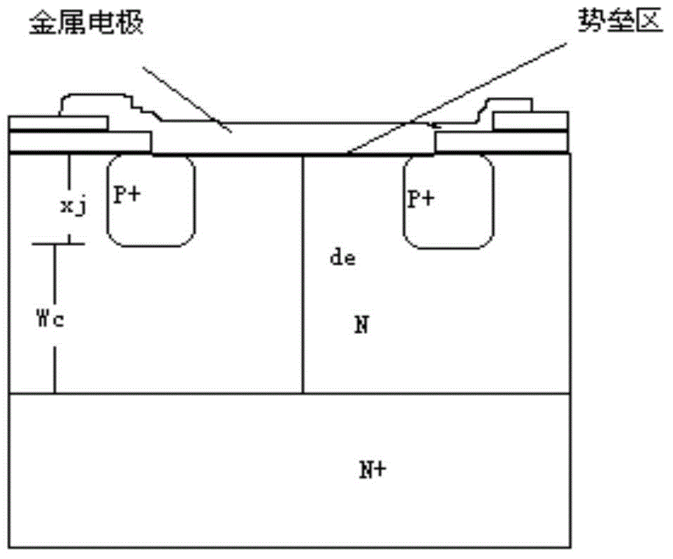
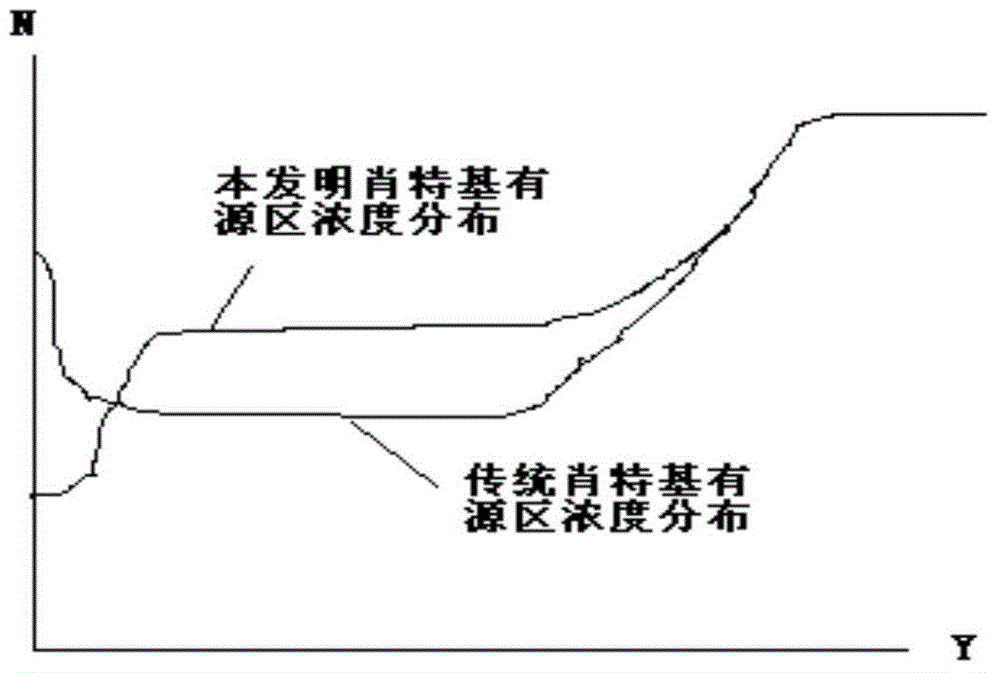
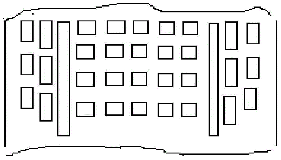
[0037] In this example, the JTE area is divided into three areas, the first area is adjacent to the active area, which is a 100% light transmission area (i.e. full injection), the second area is a 75% light transmission area, and the third area is a 50% light transmission area , the width of each area is 10um, the distance between the light-transmitting areas is 1um, and the active area is a 10% light-transmitting area. The epitaxial wafer is N+ / N type, the resistivity of N type is 0.6Ω.cm, the thickness is 4um, and the implantation dose is 3E12 / cm 2 , push junction temperature is 950℃, 60min, barrier metal is Cr, chip area is 1mm 2 .

[0038] Results: The reverse voltage is 56V (normally 48V), the reverse leakage current is 12uA (normally 35uA), and the forward voltage drop is 0.45V (normally 0.5V).


PUM


Abstract

The invention mainly aims at providing a low-electric-leakage and low-forward-voltage-drop Schottky diode structure and a manufacturing method of the low-electric-leakage and low-forward-voltage-drop Schottky diode structure. The manufacturing method is characterized in that a terminal is protected with the junction termination extension technology, neutralization modulation is carried out on Schottky main junction depletion regions at the same time, injections of the two terms are carried out at the same time, the breakdown voltage is improved, the good low-electric-leakage effect can be achieved, and the process manufacturing procedure is simple. After the low-electric-leakage and low-forward-voltage-drop Schottky diode structure and the manufacturing method are applied, a low-electrical-resistivity epitaxial wafer can be adopted for manufacturing a Schottky diode, the forward voltage drop is effectively reduced, the high-voltage effect is achieved, and the low-electric-leakage and low-forward-voltage-drop effect is improved. By means of the low-electric-leakage and low-forward-voltage-drop Schottky diode structure and the manufacturing method, the efficient Schottky barrier diode can be obtained; compared with a traditional diode structure, the application scope of the diode is wide.

Description

technical field [0001] The invention belongs to the technical field of diodes and their preparation, in particular to a Schottky diode with low leakage current and low forward voltage drop and a preparation method thereof. Background technique [0002] Schottky Barrier Diode (SBD) is widely used in DC-DC converter (DC-DC converter), voltage regulator (Voltage Regulator Module VRM), telecom transmission / server (Telecom / Server), AC Power adapter (Adaptor) and charger (Charger), etc. In all these applications, Schottky barrier diodes need to guarantee a certain breakdown voltage and low forward voltage drop and low reverse leakage current to ensure low power consumption. [0003] However, the electrical parameters of the above-mentioned devices, forward voltage drop and reverse leakage current, need a compromise, because reducing the forward voltage drop will inevitably lead to an increase in reverse leakage and a decrease in reverse voltage; It will inevitably lead to an inc...

Claims


Application Information

Patent Timeline
Patent Type & Authority Applications(China)
IPC IPC(8): H01L29/872H01L29/06H01L21/329
CPCH01L29/872H01L29/0615H01L29/0638H01L29/66143
Inventor 鲁艳春杨忠武王国峰
Owner SHANGHAI ANWEI ELECTRONICS
Why Eureka
Try Eureka