AlN film growing on Zr substrate, and preparation method and application of AlN film
A thin film and substrate technology, applied in the field of AlN thin film and its preparation, can solve the problems of unstable chemical properties of metal Zr substrate, difficulty in thin film epitaxy, affecting the quality of epitaxial thin film growth, etc., so as to improve the internal quantum efficiency and current distribution. Beneficial effect of uniformity and efficiency improvement
- Summary
- Abstract
- Description
- Claims
- Application Information
AI Technical Summary
Problems solved by technology
Method used
Image
Examples
Embodiment 1
[0034] The AlN thin film grown on the Zr substrate of the present embodiment comprises the following steps:
[0035](1) Selection of the substrate and its crystal orientation: the epitaxial substrate uses the (0001) plane of the Zr substrate as the epitaxial plane, and the selected crystal epitaxial orientation relationship: AlN(0001) / / Zr(0001).
[0036] (2) Epitaxial growth of AlN film: the substrate temperature was adjusted to 450°C, and the reaction chamber pressure was 3×10 -5 Torr, Ⅴ / Ⅲ ratio is 50, growth rate is 0.6ML / s; energy consumption is 3.0J / cm 2 And a KrF excimer laser (λ=248nm, t=20ns) PLD with a repetition rate of 20Hz ablates the AlN target (99.99wt%), and epitaxially grows an AlN film with a thickness of 200nm. When depositing AlN thin films, the growth chamber pressure N 2 (99.9999vol%) kept at 3~4×10 -5 Torr to ensure high-quality AlN films.
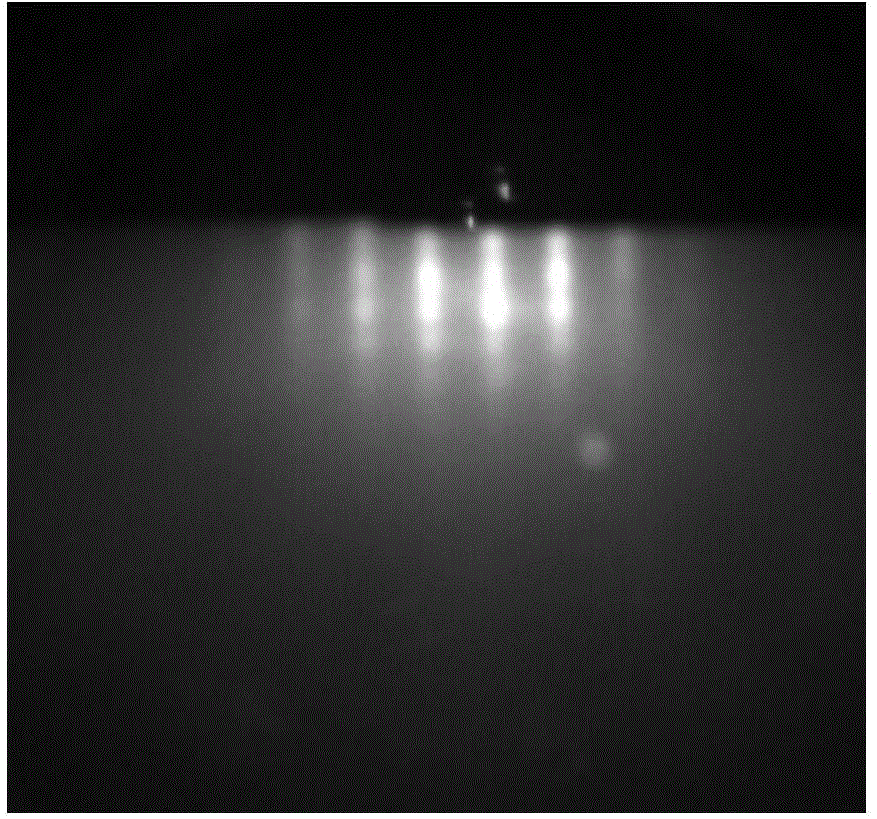
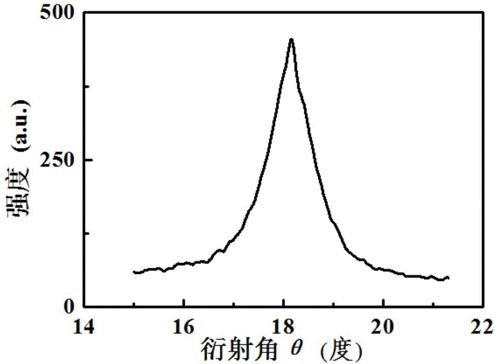
[0037] Such as figure 1 As shown, the cross-sectional schematic view of the high-quality AlN film grown on the ...
Embodiment 2
[0044] The AlN thin film grown on the Zr substrate of the present embodiment comprises the following steps:
[0045] (1) Selection of the substrate and its crystal orientation: the epitaxial substrate uses the (0001) plane of the Zr substrate as the epitaxial plane, and the selected crystal epitaxial orientation relationship: AlN(0001) / / Zr(0001).
[0046] (2) Epitaxial growth of AlN film: the substrate temperature was adjusted to 550°C, and the reaction chamber pressure was 4×10 -5 Torr, Ⅴ / Ⅲ ratio is 60, growth rate is 0.4ML / s; energy consumption is 3.0J / cm 2 And a KrF excimer laser (λ=248nm, t=20ns) PLD with a repetition rate of 20Hz ablates the AlN target (99.99wt%), and epitaxially grows an AlN film with a thickness of 20nm. When depositing AlN thin films, the growth chamber pressure N 2 (99.9999%) kept at 3~4×10 -5 Torr to ensure high-quality AlN films.
[0047] The performance of the AlN thin film grown on the Zr substrate prepared in this embodiment is similar to tha...
PUM
| Property | Measurement | Unit |
|---|---|---|
| thickness | aaaaa | aaaaa |
| thickness | aaaaa | aaaaa |
| thickness | aaaaa | aaaaa |
Abstract
Description
Claims
Application Information


