Inverted LED chip with high light emitting efficiency and LED device and manufacturing method of inverted LED chip with high light emitting efficiency

An LED chip and flip-chip technology, applied in semiconductor devices, electrical components, circuits, etc., can solve the problems of the chip's electrical and thermal conductivity, the influence of light extraction efficiency, the inability to be further improved, and the numerous manufacturing processes, so as to save process steps and manufacturing. cost, reduce material cost and process cost, and improve the effect of light extraction efficiency

Inactive Publication Date: 2014-11-05
APT ELECTRONICS
View PDF2 Cites 16 Cited by
  • Summary
  • Abstract
  • Description
  • Claims
  • Application Information

AI Technical Summary

Problems solved by technology

[0005] The existing method of making flip-chip LED chips has six main steps, and each step uses a photolithography process, which leads to high production costs due to numerous manufacturing processes
Moreover, in the flip-chip LED chip made in this way, its P contact metal layer and P barrier protection layer are all made on the stepped P-type epitaxial layer 13 by etching in the subsequent process. Due to the limitation of photolithography precision, not only The coverage area of ​​the P contact metal layer is much smaller than the surface area of ​​the P-type epitaxial layer, and the coverage area of ​​the P-blocking protective layer is also smaller than the surface area of ​​the P-type epitaxial layer, which will affect the thermal conductivity and light extraction efficiency of the chip, and cannot be obtained. further improvement

Method used


Image

  • Inverted LED chip with high light emitting efficiency and LED device and manufacturing method of inverted LED chip with high light emitting efficiency
  • Inverted LED chip with high light emitting efficiency and LED device and manufacturing method of inverted LED chip with high light emitting efficiency
  • Inverted LED chip with high light emitting efficiency and LED device and manufacturing method of inverted LED chip with high light emitting efficiency

Examples


Embodiment 1

[0060] This embodiment is an embodiment of flip-chip LED chips.

[0061] refer to image 3 , image 3 It is a schematic cross-sectional structure diagram of the flip-chip LED chip of Embodiment 1.

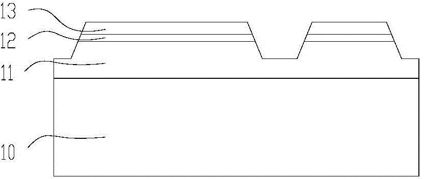
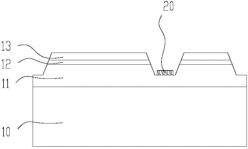
[0062] The flip-chip LED chip 600 of this embodiment includes an epitaxial substrate 100, an N-type epitaxial layer 101 superimposed on the upper surface of the epitaxial substrate layer 100, a light-emitting layer 102 superimposed on the upper surface of the N-type epitaxial layer 101, and a light-emitting layer superimposed on the light-emitting layer 100. P-type epitaxial layer 103 on the upper surface of layer 102 . Wherein, a first concave hole 502 is opened on the upper surface of the P-type epitaxial layer 103, the first concave hole 502 penetrates through the light-emitting layer 102, and extends downward to the N-type epitaxial layer 101, and the first concave hole 502 does not completely penetrate The N-type epitaxial layer 101. A P-contact metal layer 201 is stacked ...

Embodiment 2

[0068] see Figure 5 , this embodiment is an embodiment of an LED device formed by flip-chip mounting the flip-chip LED chip 600 on the substrate 300 in Embodiment 1.

[0069] see Figure 5, which is a schematic structural diagram of the LED device of this embodiment. The LED device includes a substrate 300 and a flip-chip LED chip 600 flip-chip mounted on the substrate 300 . The flip-chip LED chip is the flip-chip LED chip provided in Embodiment 1. The substrate 300 is provided with P electrodes 301 and N electrodes 302 spaced apart from each other, and the P surface electrodes 204 and N surface electrodes 205 of the flip-chip LED chip 600 are respectively connected to the P electrodes 301 and N electrodes 302 on the substrate 300 for connection. The method is an existing method in the technical field such as reflow soldering, ultrasonic thermocompression welding, or pasting with conductive adhesive. More preferably, the substrate 300 is provided with a third through hole...

Embodiment 3

[0073] see Figure 6 , this embodiment is an embodiment of an LED device formed by flip-chip mounting the flip-chip LED chip 600 on the substrate 400 in Embodiment 1.

[0074] see Figure 6 , which is a schematic structural diagram of the LED device of this embodiment. The LED device includes a substrate 400 and at least one flip-chip LED chip 600 provided in Embodiment 1. The surface of the substrate 400 is provided with a plurality of substrate electrodes 401 , and adjacent substrate electrodes 401 are spaced apart. The substrate electrode 401 is used for electrical connection with the flip-chip LED chip 600 and external devices. Specifically, when the flip-chip LED chip 600 is flip-chip connected to the substrate 400 , its P surface electrode 204 and N surface electrode 205 are respectively connected to two adjacent substrate electrodes 401 .

[0075] Through the electrical connection of the substrate electrodes 401, a plurality of flip-chip LED chips 600 will form a se...


PUM


Abstract

The invention provides an inverted LED chip, a manufacturing method of the inverted LED chip and an LED device comprising the inverted LED chip. A first concave hole is formed in a P-type epitaxial layer of the inverted LED chip; a P-type contact metal layer is overlapped to the upper surface of the P-type epitaxial layer; a P-type blocking protective layer is overlapped to the upper surface of a first overlapping structure, and the coverage area of the lower surface of the P-type blocking protective layer is coincident with the area of the upper surface of the P-type epitaxial layer; an insulating layer is arranged on the exposed surface of a second overlapping structure, a first through hole is formed in the part, corresponding to the position of the bottom of the first concave hole, of the insulating layer of the second overlapping structure, and a second through hole is formed in the part, corresponding to the upper surface of the P-type blocking protective layer, of the insulating layer of the second overlapping structure; an N-type surface electrode is electrically connected with an N-type epitaxial layer through the first through hole, and a P-type surface electrode is electrically connected with the P-type blocking protective layer through the second through hole. By means of the inverted LED chip, the heat conduction capacity and the electric conduction capacity are good, and the light emitting efficiency is easily improved.

Description

technical field [0001] The invention belongs to the field of manufacturing light-emitting devices, and relates to a structure of a light-emitting diode chip and a manufacturing method thereof, in particular to a flip-chip light-emitting diode chip and a manufacturing method thereof, and an LED device containing the flip-chip LED chip. Background technique [0002] Light-emitting diode (LED) light sources have the advantages of high efficiency, long life, and no harmful substances such as Hg. With the rapid development of LED technology, the brightness and lifespan of LEDs have been greatly improved, making the application of LEDs more and more extensive. From outdoor lighting such as street lights to urban lighting such as decorative lights, they are all used or Replace with LED as light source. [0003] In the semiconductor lighting industry, the structure of LED chips is generally divided into three types: front chip structure, vertical chip structure and flip chip struct...

Claims


Application Information

Patent Timeline
Patent Type & Authority Applications(China)
IPC IPC(8): H01L33/38H01L33/00
CPCH01L33/382H01L2933/0016
Inventor 许朝军姜志荣曾照明黄靓肖国伟
Owner APT ELECTRONICS
Why Eureka
Try Eureka