Preparation technology of high-density interconnecting printed circuit board

A printed circuit board, high-density interconnection technology, applied in the direction of printed circuit, printed circuit manufacturing, printed circuit secondary processing, etc., can solve the problems of waste of raw materials, increased production cost, increased production cost, etc., to improve accuracy and Thickness uniformity, work efficiency improvement, and time-saving effects

Inactive Publication Date: 2014-11-05
SHANGHAI MEADVILLE ELECTRONICS +1
View PDF6 Cites 5 Cited by
  • Summary
  • Abstract
  • Description
  • Claims
  • Application Information

AI Technical Summary

Problems solved by technology

Since the via hole is filled by electroplating the entire board, a certain thickness of electroplated metal is also deposited on the surface copper foil. If the thickness value is too small, fine lines cannot be made, and it is necessary to perform etching again to reduce the thickness of the copper foil. It is suitable for the production of thin lines, and the process is cumbersome.
On the other hand, due to the process of etching and thinning the surface copper thickness, increasing the thickness by electroplating deposition, and then etching and thinning the surface copper thickness, the thickness uniformity of the conductive layer will be greatly reduced, and the greater the amount of side etching and the greater the amount of electroplating, the greater the amount of etching. The lower the accuracy and plating accuracy, the worse the thickness uniformity, which directly affects the circuit manufacturing capability and tolerance accuracy, and greatly reduces the quality and pass rate of high-density interconnection circuit boards
Therefore, it cannot meet the development requirements of lighter, smaller and thinner electronic products
In addition, in order to avoid the influence of etching thinning and electroplating deposition on the uniformity of copper thickness in the traditional process, only by increasing the production capacity of etching and electroplating equipment and improving the management and control of production can it be possible to reduce the impact of etching and electroplating on the conductive layer. The influence of thickness uniformity, but the production cost will be greatly increased
Etching and thinning copper foil will also cause waste of raw materials and increase production costs

Method used


Image

  • Preparation technology of high-density interconnecting printed circuit board
  • Preparation technology of high-density interconnecting printed circuit board
  • Preparation technology of high-density interconnecting printed circuit board

Examples


Embodiment Construction

[0036] The present invention is described in detail below in conjunction with accompanying drawing:

[0037] The manufacturing process of high-density interconnection printed circuit board is characterized in that it includes:

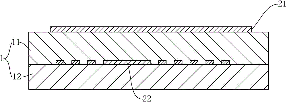
[0038] a. If figure 1 As shown, a first substrate 1 is provided. The first substrate 1 includes two first insulating layers, namely a first insulating layer 11 and a first insulating layer 12 . A first conductive layer 21 is provided on the upper surface of the first insulating layer 11 , and a second conductive circuit 22 is provided between the first insulating layer 11 and the first insulating layer 12 . The first conductive layer 21 is copper foil with a thickness of 15 μm.

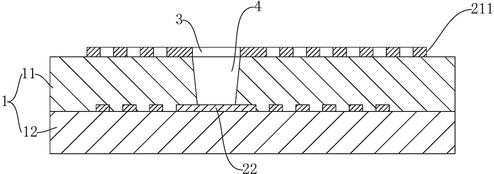
[0039] b. If figure 2As shown, the first conductive layer 21 is etched with an etchant to form a first conductive circuit 211 with a line width / space of 40 μm / 40 μm and a first window 3 . The first window 3 is a circular hole with a diameter of 50 μm.
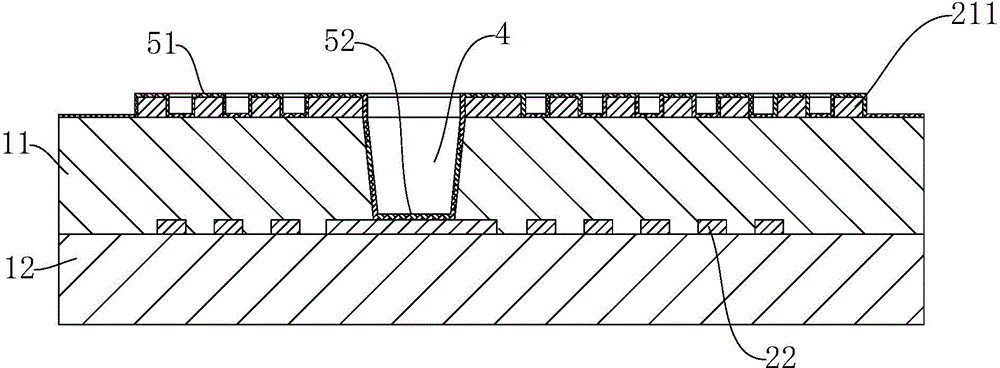
[0040] c. Drilli...


PUM

PropertyMeasurementUnit
thicknessaaaaaaaaaa
widthaaaaaaaaaa
distanceaaaaaaaaaa

Abstract

The invention discloses a preparation technology of a high-density interconnecting printed circuit board. The preparation technology is characterized by comprising the steps of providing a first substrate which comprises a first conducting layer, a second conducting circuit and first insulating layers, etching the first conducting layer to form a first conducting circuit and a first window, drilling one first insulating layer to form a through hole, performing chemical copper deposition treatment on the first substrate, arranging a protective film on the surface of metallic copper covering the upper surface of the first substrate, forming a second window corresponding to the first window in the protective film, performing electroplating treatment on the first substrate provided with the protective film to allow the through hole and the first window to be filled with metallic copper, removing the protective film, and removing the metallic copper covering the upper surface of one first insulating layer, wherein the first conducting layer is located on the surface of one first insulating layer. The preparation technology of the high-density interconnecting printed circuit board saves a procedure of etching to reduce the thickness of the conducting circuits, improves the accuracy and the thickness uniformity of the conducting circuits, and improves the quality of the high-density interconnecting circuit board.

Description

technical field [0001] The invention relates to the field of printed circuit board manufacturing, in particular to a manufacturing process of an inner layer board of a high-density interconnected printed circuit board. Background technique [0002] As the main support for the installation and insertion of electronic components, the circuit board is an indispensable part of all electronic products. In recent years, the information, communication, and consumer electronics manufacturing industries have become one of the fastest growing industries in the world. Electronic products are changing with each passing day, and are constantly developing in the direction of small size, light weight, and complex functions. This puts forward more requirements for circuit boards. high demands. The traditional circuit board manufacturing process increases the circuit density of the board by reducing the line width or line spacing of the conductive lines on the board surface, so as to adapt ...

Claims


Application Information

Patent Timeline
Patent Type & Authority Applications(China)
IPC IPC(8): H05K3/00H05K3/46H05K3/28
Inventor 黄伟武瑞黄樊泽杰陶伟良
Owner SHANGHAI MEADVILLE ELECTRONICS
Why Eureka
Try Eureka