
Conductive plug and TSV forming method

A technology of conductive plugs and semiconductors, which is applied in the manufacture of circuits, electrical components, semiconductors/solid-state devices, etc., and can solve problems affecting the stability of TSV conduction, etc.

Inactive Publication Date: 2014-11-12
SEMICON MFG INT (SHANGHAI) CORP
View PDF5 Cites 7 Cited by
  • Summary
  • Abstract
  • Description
  • Claims
  • Application Information

AI Technical Summary

Problems solved by technology

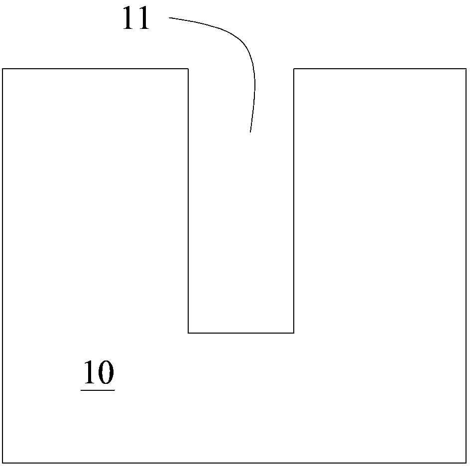
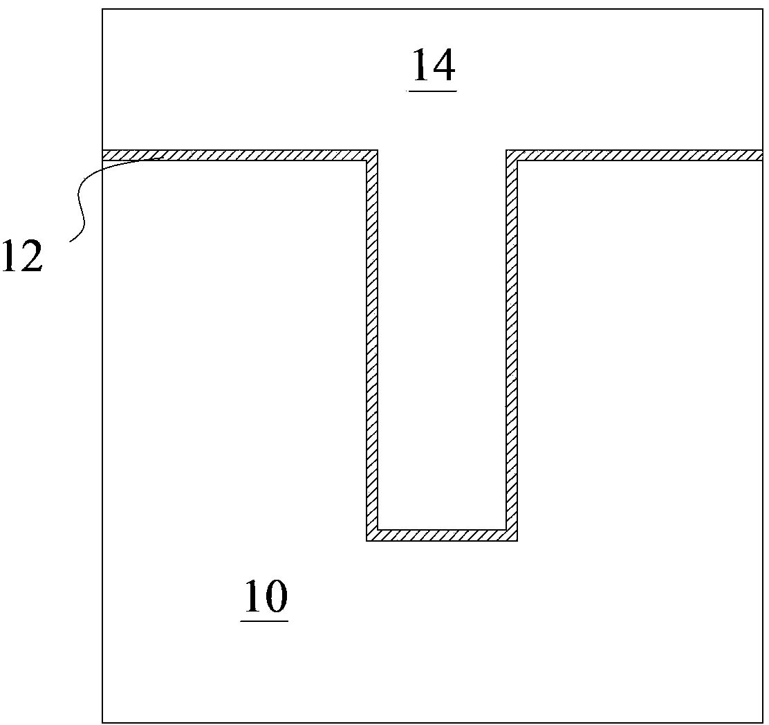
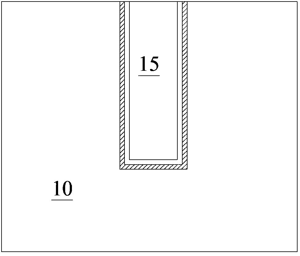
[0006] However, in actual operation, it is found that after the annealing process, the connection interface between the metal conductive layer 14 and the insulating layer 12, and even between the insulating layer 12 and the substrate 10, cracks of varying degrees will appear, thereby affecting the conductive stability of the formed TSV. , and the stability of the resulting semiconductor device

Method used


Image

  • Conductive plug and TSV forming method
  • Conductive plug and TSV forming method
  • Conductive plug and TSV forming method

Examples


Embodiment 1

[0049] refer to figure 2 As shown, a semiconductor substrate 100 is provided, and the semiconductor substrate 100 includes an upper surface 200 and a lower surface 300 . The material of the semiconductor substrate 100 can be silicon, germanium, gallium arsenide or silicon germanium compound. Existing semiconductor substrates can all be used as the semiconductor substrate 100 of the present invention, and will not be listed here. In this embodiment, the semiconductor substrate 100 is preferably made of silicon.

[0050] refer to image 3 As shown, the semiconductor substrate 100 is etched to form a blind hole 110 in the semiconductor substrate 100 . The specific process includes: coating a hard mask layer 101 on the upper surface 200 of the semiconductor substrate 100, and patterning the hard mask layer 101 by a process such as photolithography, and forming in the hard mask layer 101 Opening (marked in figure). Afterwards, using the patterned hard mask layer 101 as a mask...

Embodiment 2

[0065] The method for forming the conductive plug provided in this embodiment is substantially the same as the technical solution of the method for forming the conductive plug provided in Embodiment 1, the only difference being that before the annealing process, the CMP process is used to remove the covering on the semiconductor substrate 100. The entire thickness of the upper surface of the metal layer 104 further ensures that the stress generated in the semiconductor substrate 100 , the metal layer 104 , the metal shielding layer 103 and the insulating layer 102 during the annealing process is fully released.

[0066] After the conductive plug 106 is formed as in Embodiment 1 and Embodiment 2, refer to Figure 8 As shown, the lower surface 300 of the semiconductor substrate 100 is polished by a process such as CMP, so that the conductive plug 106 is connected to the blind hole 110 to form a TSV in the semiconductor substrate 100 . And in the subsequent packaging process, the...


PUM

PropertyMeasurementUnit
Thicknessaaaaaaaaaa
Thicknessaaaaaaaaaa

Abstract

The invention provides a conductive plug and TSV forming method. The conductive plug forming method includes the steps that a blind hole is formed in a semiconductor substrate, after metal layers are formed in the blind hole and formed on the semiconductor substrate, the metal layer, of the part of the full thickness, on the semiconductor substrate is removed first, and the substrate is heated by adopting the annealing technology, so that refinement, regrowth and homogenization of crystalline grains in the metal layers are achieved, and the internal structure of the metal layers is optimized. After the metal layer, of the part of the full thickness, on the semiconductor substrate is removed, while stress generated by deformation of the metal layers in the annealing process can be effectively reduced, stress generated by volume deformation, based on heat-expansion and cold-contraction, of the semiconductor substrate and structures on all the layers on the semiconductor substrate is fully released, acting force between the substrate and the structures on all the layers is reduced, and cracks on the connection faces between the semiconductor substrate and the structures on all the layers in the semiconductor substrate are avoided.

Description

technical field [0001] The invention relates to the field of semiconductor formation, in particular to a method for forming a conductive plug and a TSV. Background technique [0002] With the rapid development of the information industry, the feature size (CD) of integrated circuits has been continuously reduced, and the manufacturing process of integrated circuit chips has also been miniaturized. The development of integrated circuit chip preparation technology has prompted integrated circuit packaging technology to continuously pursue the demand for higher performance, more functions, smaller size, lower power consumption and cost. [0003] In the development of integrated circuit packaging technology, 3D TSV (Through-Silicon-Via) packaging technology realizes the interconnection between chips by making vertical conduction between chips and between wafers. of the latest technology. Compared with the previous IC package bonding and overlay technology using bumps, TSV can ...

Claims


Application Information

Patent Timeline
IPC IPC(8): H01L21/768
CPCH01L21/76897H01L21/76898
Inventor 孙光宇
Owner SEMICON MFG INT (SHANGHAI) CORP
Learn More