Plasma nitrogen treatment apparatus, and gate medium layer preparation method and device

A technology of plasma nitriding and processing equipment, which is applied in the manufacture of semiconductor/solid-state devices, discharge tubes, electrical components, etc., to achieve the effect of improving the bonding rate, promoting amorphization, and reducing the diffusion effect

Inactive Publication Date: 2014-11-19
SHANGHAI HUALI MICROELECTRONICS CORP
View PDF6 Cites 5 Cited by
  • Summary
  • Abstract
  • Description
  • Claims
  • Application Information

AI Technical Summary

Problems solved by technology

[0010] However, in the above preparation process, since the nitrogen plasma is still injected into the silicon dioxide layer at a certain speed and energy, if the degree of plasma damage is too large, it is difficult to repair by PNA high temperature annealing

Method used


Image

  • Plasma nitrogen treatment apparatus, and gate medium layer preparation method and device
  • Plasma nitrogen treatment apparatus, and gate medium layer preparation method and device
  • Plasma nitrogen treatment apparatus, and gate medium layer preparation method and device

Examples


Embodiment Construction

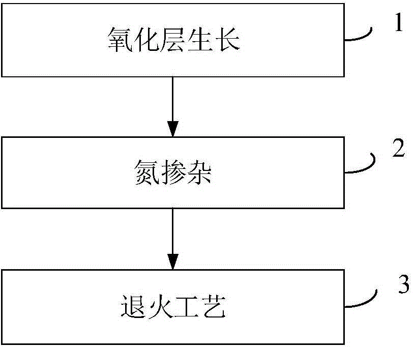
[0031] In order to make the content of the present invention clearer and easier to understand, the content of the present invention will be further described below in conjunction with the accompanying drawings. Of course, the present invention is not limited to this specific embodiment, and general replacements known to those skilled in the art are also covered within the protection scope of the present invention.

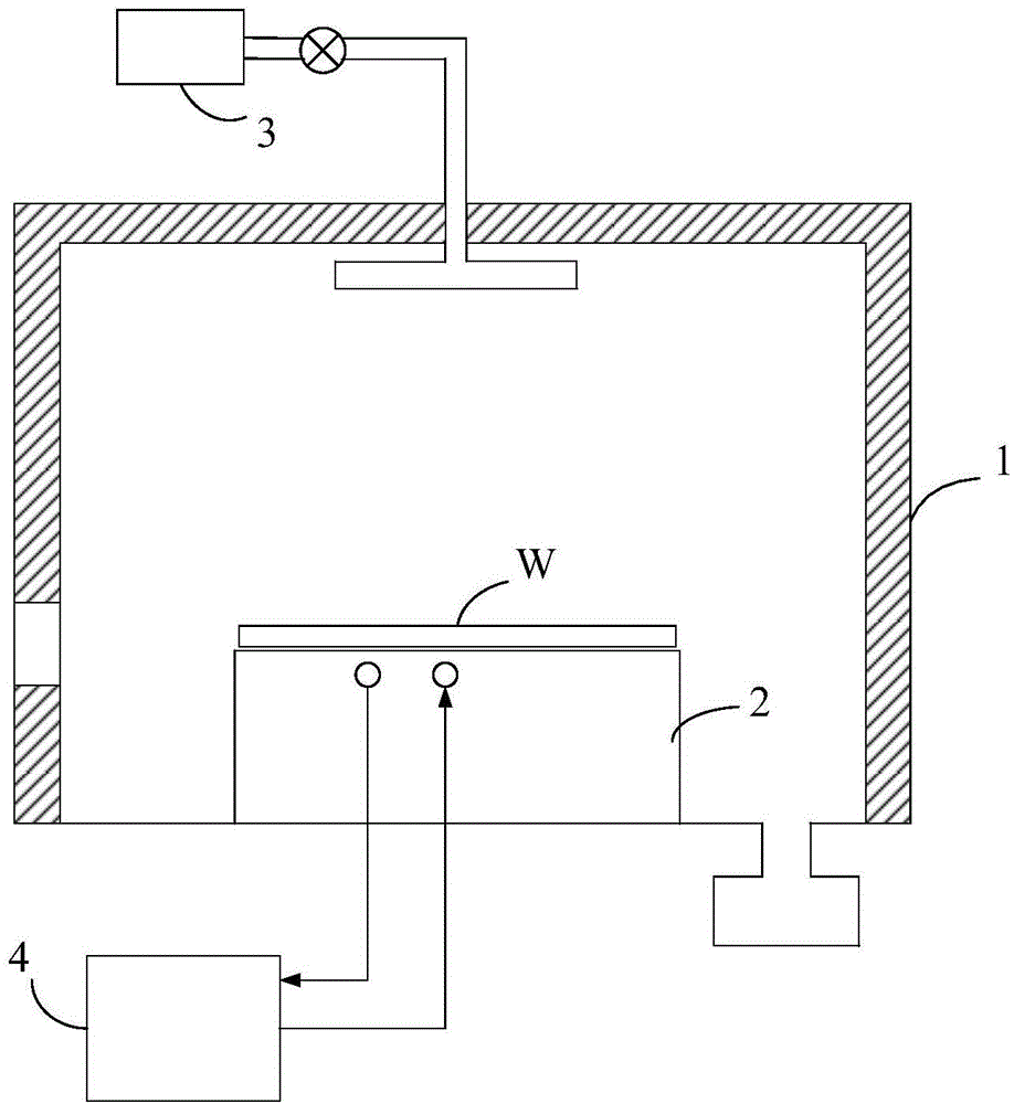
[0032] figure 2 A plasma nitriding treatment device according to an embodiment of the present invention is shown, which is a decoupled plasma nitriding treatment device and can be used to implement plasma nitrogen implantation on a silicon dioxide film on a substrate. It should be understood that the plasma nitriding treatment device is only is exemplary, it may include fewer or more constituent elements, or the arrangement of the constituent elements may be the same as or different from that shown in the drawings.

[0033] See figure 2, The plasma nitriding tr...


PUM


Abstract

The invention discloses a plasma nitrogen treatment apparatus. The plasma nitrogen treatment apparatus comprises a vacuum treatment cavity for supporting a pedestal of a substrate with a silicon dioxide film, a gas supply mechanism for supplying a nitrogen-containing gas to the vacuum treatment cavity, a plasma generating mechanism for ionizing the nitrogen-containing gas to nitrogen plasma, and a cooling mechanism for cooling the pedestal to -100 DEG C to 0 DEG C before injecting the nitrogen plasma in the silicon dioxide film. The invention also provides a gate medium layer preparation device with the plasma nitrogen treatment apparatus, and a corresponding gate medium layer preparation method. According to the invention, the reliability of a gate medium layer can be effectively improved.

Description

technical field [0001] The invention relates to the technical field of semiconductor manufacturing, in particular to a plasma nitriding treatment device, equipment and method for making a gate dielectric layer. Background technique [0002] Integrated circuits are made up of millions of basic building blocks such as transistors, capacitors and resistors. A transistor usually includes a source, a drain, and a gate stack, and the composition of the gate stack is to form a dielectric layer (usually silicon dioxide) above the substrate, and then cover a thin film as an electrode on the dielectric layer ( such as polysilicon). [0003] With the rapid development of very large-scale integrated circuits (VLSI) and ultra-large-scale integrated circuits (ULSI), the size of MOS devices is continuously reduced. The thickness of the silicon gate dielectric layer is continuously reduced. However, as the thickness of the silicon dioxide gate dielectric layer is reduced, there are some ...

Claims


Application Information

Patent Timeline
Patent Type & Authority Applications(China)
IPC IPC(8): H01L21/67H01L21/28H01J37/32
CPCH01L21/67213H01L21/28185H01L21/28202H01L21/6719
Inventor 肖天金康俊龙余德钦
Owner SHANGHAI HUALI MICROELECTRONICS CORP
Why Eureka
Try Eureka