Terahertz modulator, system and method based on silicon-based microstructure on soi

A silicon-based microstructure, terahertz detector technology, applied in the field of terahertz technology and applications, can solve the problems of unfavorable terahertz imaging accuracy, high terahertz wave insertion loss, low sensitivity, etc., to improve resolution and reduce load. The effect of carrier diffusion, the effect of enhancing transmittance

Active Publication Date: 2021-07-02
UNIV OF ELECTRONICS SCI & TECH OF CHINA
View PDF6 Cites 0 Cited by
  • Summary
  • Abstract
  • Description
  • Claims
  • Application Information

AI Technical Summary

Problems solved by technology

[0004] There are three main problems in traditional optically controlled terahertz modulators. One is that the insertion loss of terahertz waves is too high, and the reflection of terahertz waves by traditional high-resistance silicon terahertz modulators is as high as 30%. The power is generally low, and the sensitivity of the terahertz detector is relatively low, which is a great loss. In 2014, Yan Peng, XiaoFei Zang and others prepared a terahertz detector based on a double-layer doped silicon grating structure. The perfect absorber excites the air-gap mode resonance through a grating array. After a series of parameter optimization, it finally achieves an absorption rate of 95% for terahertz waves, that is, only 5% for terahertz wave reflections, effectively solving the problem of terahertz waves. The insertion loss problem in wave transmission; the second is the modulation depth problem. The modulation depth of the current traditional silicon-based optically controlled terahertz amplitude modulator is relatively low, which is difficult to meet the requirements of the current terahertz imaging system; the third is the carrier diffusion The problem is that when the modulated laser light of the optically controlled terahertz modulator is incident on the surface of the modulator, the photogenerated carriers will diffuse around the modulated laser signal, resulting in a larger corresponding area, which is not conducive to the improvement of terahertz imaging accuracy.

Method used


Image

  • Terahertz modulator, system and method based on silicon-based microstructure on soi
  • Terahertz modulator, system and method based on silicon-based microstructure on soi
  • Terahertz modulator, system and method based on silicon-based microstructure on soi

Examples


Embodiment 1

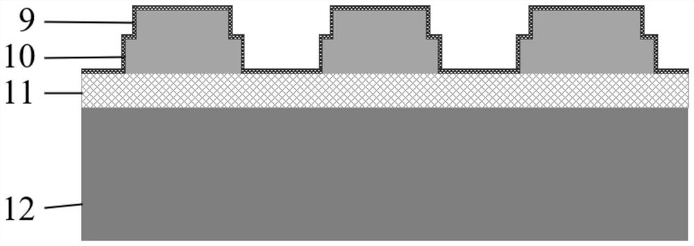
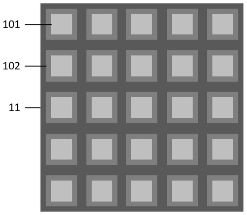
[0042] Such as figure 2 and image 3 As shown, a terahertz modulator based on a silicon-based microstructure on SOI, including from bottom to top: the underlying Al 2 o 3 Substrate 12, SiO 2 Isolation layer 11, silicon-based microstructure 10, Al 2 o 3 Passivation layer 9, silicon-based microstructures 10 are periodically arranged on the SiO2 isolation layer 11, each silicon-based microstructure 10 includes two layers of square Si-based step structures, and from top to bottom are the upper Si-based step 101 and the lower Si-based step structure respectively. The centers of the upper Si-based step 101 and the lower Si-based step 102 of the base step 102 are aligned, and the side length of the upper Si-based step 101 is smaller than the side length of the lower Si-based step 102 .

[0043] In this embodiment, the two layers of square Si-based stepped structures of the silicon-based microstructure 10 are both Si layers, the resistivity of the Si layer is greater than 3000Ω....

Embodiment 2

[0051] Such as Figure 5 As shown, the preparation method of the terahertz modulator based on the silicon-based microstructure on SOI in Example 1 includes the following steps:

[0052] Step 1: Use the electromagnetic simulation software CST Microwave Studio to carry out 3D modeling of the silicon-based microstructure. The total thickness of the model is 500 μm, and the thickness of the Si layer is 90 μm. After setting the boundary conditions and solver, the edges of the two-layer square steps The length and step height are set as variables to scan to obtain the best simulation parameters. The best parameters obtained by final optimization are the upper Si-based steps have a side length of 66 μm and a height of 45 μm; the lower Si-based steps have a side length of 84 μm and a height of 45 μm;

[0053] Step 2: Clean the SOI substrate: first put the SOI substrate into a beaker filled with acetone for ultrasonic cleaning for 10-15 minutes, then use alcohol for ultrasonic cleaning...

Embodiment 3

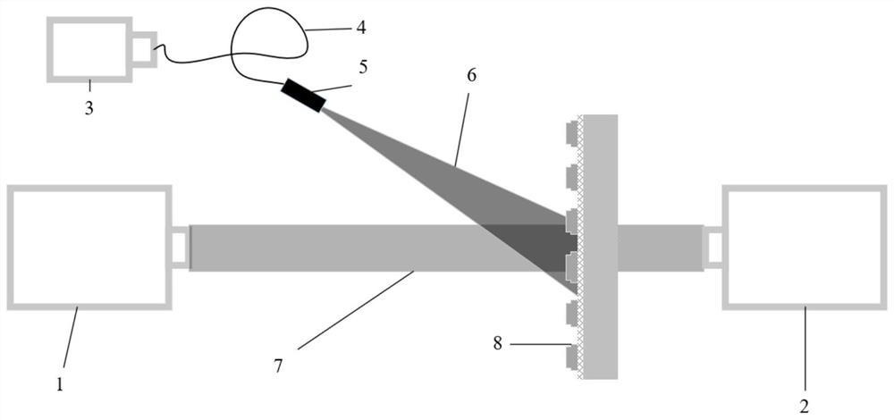
[0057] Such as figure 1 As shown, an optically controlled terahertz modulation system based on silicon-based microstructure on SOI includes: semiconductor laser 3, laser modulator 5, terahertz modulator 8, terahertz radiation source 1, terahertz detector 2, semiconductor The laser 3 is connected to the laser modulator 5 through the optical fiber 4, the laser beam 6 emitted by the laser modulator 5 is incident on the surface of the terahertz modulator 8 as the excitation laser, and the terahertz radiation source 1 and the terahertz detector 2 are located on the left and right sides of the terahertz modulator On both sides, the terahertz beam 7 emitted by the terahertz radiation source 1 passes through the terahertz modulator 8 vertically and then enters the terahertz detector 2. The incident direction of the terahertz beam 7 is that the terahertz modulator 8 has a silicon-based microstructure On one side of 10, the terahertz radiation source 1 and the terahertz detector 2 are a...


PUM

PropertyMeasurementUnit
electrical resistivityaaaaaaaaaa
thicknessaaaaaaaaaa
reflectanceaaaaaaaaaa

Abstract

The present invention provides a terahertz modulator based on a silicon-based microstructure on SOI and its preparation method and modulation system. The terahertz modulator includes from bottom to top: the underlying Al 2 o 3 Substrate, SiO 2 Isolation layer, silicon-based microstructure, Al 2 o 3 passivation layer, silicon-based microstructure in SiO 2 Periodically arranged on the isolation layer, each silicon-based microstructure includes two layers of square Si-based step structures, and the modulation system includes: a semiconductor laser, a laser modulator, a terahertz modulator, a terahertz radiation source, and a terahertz detector. The present invention For terahertz waves from 0.4THz to 0.85THz, the reflectivity is below 22%, reaching the lowest 18% at 0.82THz, which can significantly reduce the reflectivity of modulation devices to terahertz waves and improve the utilization of terahertz waves; in power Under the irradiation of 1200mw 808nm laser, the modulation depth reaches 64.5%. Compared with the traditional silicon-based terahertz modulator, the terahertz imaging diffusion area effectively improves the resolution in the imaging system to more than 21.9%.

Description

technical field [0001] The invention belongs to the field of terahertz technology and application, and relates to a terahertz amplitude modulation device in a terahertz imaging system and related fields, specifically a terahertz modulator based on a silicon-based microstructure on SOI and a preparation method thereof, and a terahertz modulator based on a silicon-based microstructure on SOI. Optically controlled terahertz modulation system with silicon-based microstructures. Background technique [0002] Terahertz refers to electromagnetic waves with a frequency ranging from 0.1 THz to 10 THz and a wavelength ranging from 0.03 mm to 3 mm. Compared with X-rays, terahertz waves can penetrate many non-polar materials and dielectric materials well, and can perform perspective imaging on opaque objects; the photon energy of terahertz radiation is only on the order of millielectronvolts (meV), less than The bond energy of various chemical bonds cannot cause various harmful ionizat...

Claims


Application Information

Patent Timeline
Patent Type & Authority Patents(China)
IPC IPC(8): G02F1/01
CPCG02F1/0102G02F2203/13
Inventor 文岐业张豪申朝阳何雨莲杨青慧谭为冯正张怀武
Owner UNIV OF ELECTRONICS SCI & TECH OF CHINA
Why Eureka
Try Eureka