A vertical gate-around tunneling transistor and its manufacturing method

A transistor and field effect transistor technology, applied in the field of gate-all-around transistors and their preparation, can solve the problems of complex GAA source-drain design, and achieve the effects of solving thermal stability problems, reducing thermal budget, and small sub-threshold slope.

Active Publication Date: 2017-06-27
PEKING UNIV
View PDF5 Cites 0 Cited by
  • Summary
  • Abstract
  • Description
  • Claims
  • Application Information

AI Technical Summary

Problems solved by technology

In addition, the introduction of nanowires makes the source and drain design of GAA more complex than planar devices and multi-gate devices

Method used


Image

  • A vertical gate-around tunneling transistor and its manufacturing method
  • A vertical gate-around tunneling transistor and its manufacturing method
  • A vertical gate-around tunneling transistor and its manufacturing method

Examples


Embodiment Construction

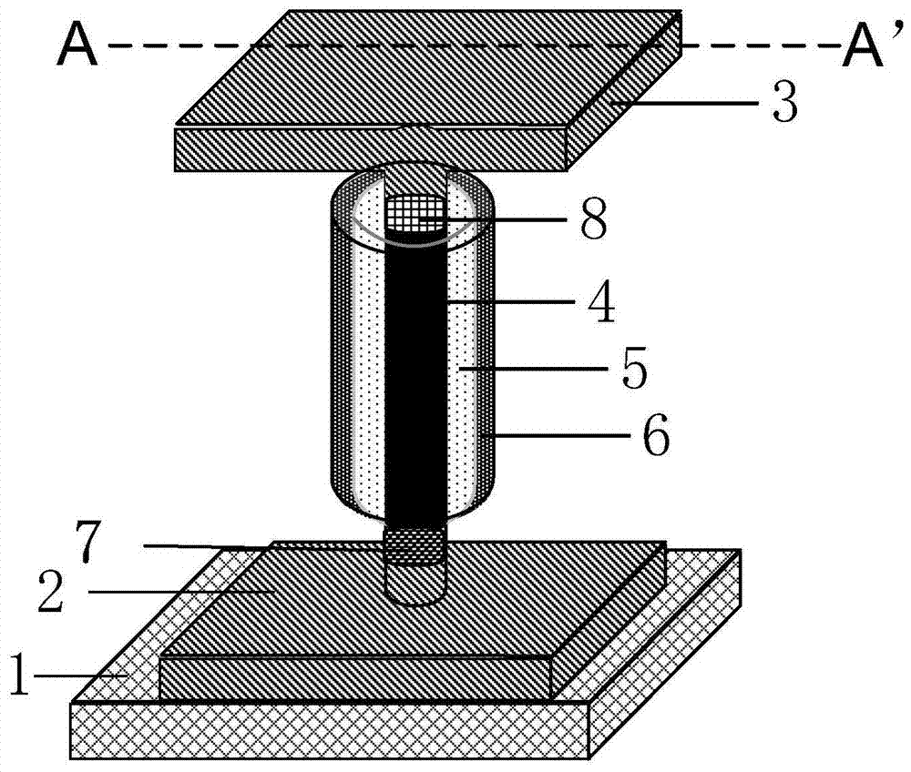
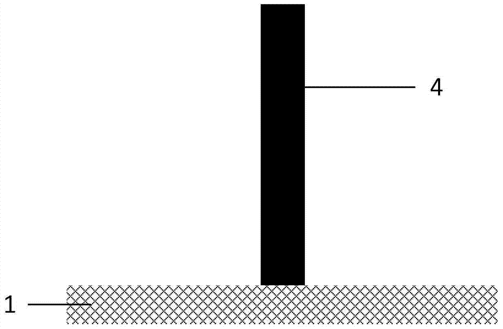
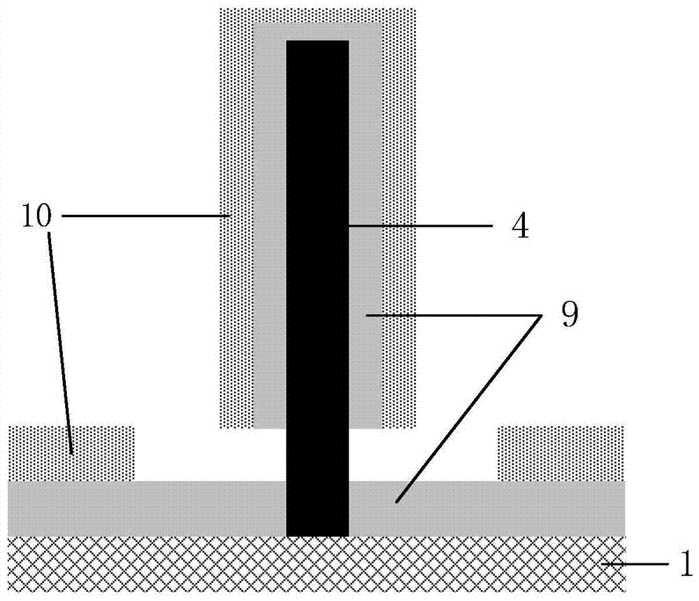
[0045] The present invention provides a field effect transistor with a novel structure, specifically a gate-all-around MOS transistor (such as figure 1 shown), including a ring-shaped semiconductor channel 4 in a vertical direction, a ring-shaped gate electrode 6, a ring-shaped gate dielectric layer 5, a source region 2, an impurity segregation region 7 (such as n-type), and a drain Region 3, an impurity segregation region 8 (different from the source region, such as p-type), a semiconductor substrate 1; wherein, the source region 2 is located at the bottom of the vertical channel 4, connected to the substrate 1, and the impurity segregation Region 7 is between source region 2 and vertical channel 4; drain region 3 is located at the top of vertical channel 4, impurity segregation region 8 is between drain region 3 and vertical channel 4; gate dielectric layer 5 and gate The electrode 6 surrounds the vertical channel 4 in a ring shape; the source region 2 and the drain region 3...


PUM


Abstract

The invention provides an around-gate field effect transistor which combines a vertical channel, heterogeneous impurity segregation and a schottky barrier source / drain structure. The around-gate field effect transistor comprises an annular semiconductor channel in the vertical direction, an annular gate electrode, an annular gate dielectric layer, a source region, an impurity segregation region (7), a drain region, an impurity segregation region (8), and a semiconductor substrate, wherein the source region is located at the bottom part of the vertical channel and connected with the substrate, and the impurity segregation region (7) is located between eth source region and the vertical channel; the drain region is located at the top part of the vertical channel, and the impurity segregation region (8) is located between the drain region and the vertical channel; the gate dielectric layer and the gate electrode surround the vertical channel; schottky contact is formed respectively between the source region and the drain region and the channel; and impurities of the impurity segregation region (7) and the impurity segregation region (8) choose heterogeneous impurities, that is, impurities of the impurity segregation region (7) choose p-type material, and impurities of the impurity segregation region (8) choose n-type material; and impurities of the impurity segregation region (7) choose n-type material, and impurities of the impurity segregation region (8) choose p-type material.

Description

technical field [0001] The invention belongs to the field of field effect transistor logic devices and circuits in CMOS ultra-large integrated circuits (ULSI), and in particular relates to a gate-all-around transistor combined with vertical channels, heterogeneous impurity segregation and Schottky barrier source / drain structures and its Preparation. Background technique [0002] Driven by Moore's Law, the feature size of traditional MOSFETs has been shrinking, and now it has entered the nanometer scale. As a result, the negative effects of short-channel effects on devices have become more serious. The effects of leakage-induced barrier reduction and band-band tunneling increase the off-state leakage current of the device. In the research on new device structures, the source-drain doped Gate All Around transistor (GAA) structure is currently the most concerned one. GAA devices have better gate control characteristics, which can meet the sharpest characteristic requirements,...

Claims


Application Information

Patent Timeline
Patent Type & Authority Patents(China)
IPC IPC(8): H01L29/78H01L29/423H01L21/336
CPCH01L29/0607H01L29/1037H01L29/36H01L29/4236H01L29/66666H01L29/7827H01L29/7839
Inventor 孙雷徐浩张一博韩静文王漪张盛东
Owner PEKING UNIV
Why Eureka
Try Eureka