Semiconductor device and manufacturing method thereof

A manufacturing method and semiconductor technology, applied in semiconductor/solid-state device manufacturing, semiconductor devices, electrical components, etc., can solve problems such as large gate-source parasitic capacitance and parasitic on-resistance, and reduce parasitic resistance effects and parasitic on-resistance. Capacitance effect, high reliability effect

Active Publication Date: 2014-11-19
GPOWER SEMICON
View PDF4 Cites 23 Cited by
  • Summary
  • Abstract
  • Description
  • Claims
  • Application Information

AI Technical Summary

Problems solved by technology

[0006] Another improved field plate technology is to divide the connecting part of the source field plate and the source into several segments, and reduce the source field plate metal and the gate and the two-dimensional electron gas conduction channel on the basis of satisfying the electrical connection of the source field plate. The overlapping area of ​​the channel, the top view of the device structure is as follows figure 2 As shown, but in this technology, the distance between the source field plate and the gate and the two-dimensional electron gas conduction channel is still very close, and a large gate-source parasitic capacitance and parasitic on-resistance will still be generated.

Method used


Image

  • Semiconductor device and manufacturing method thereof
  • Semiconductor device and manufacturing method thereof
  • Semiconductor device and manufacturing method thereof

Examples


Embodiment Construction

[0061] The present invention will be described in detail below in conjunction with specific embodiments shown in the accompanying drawings. However, these embodiments do not limit the present invention, and any structural, method, or functional changes made by those skilled in the art according to these embodiments are included in the protection scope of the present invention.

[0062] Furthermore, repeated reference numerals or designations may be used in different embodiments. These repetitions are merely for the sake of simplicity and clarity of describing the present invention, and do not imply any relationship between the different embodiments or structures discussed.

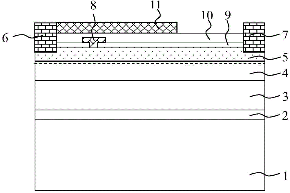
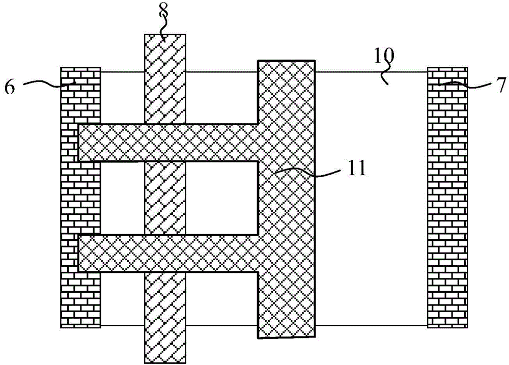
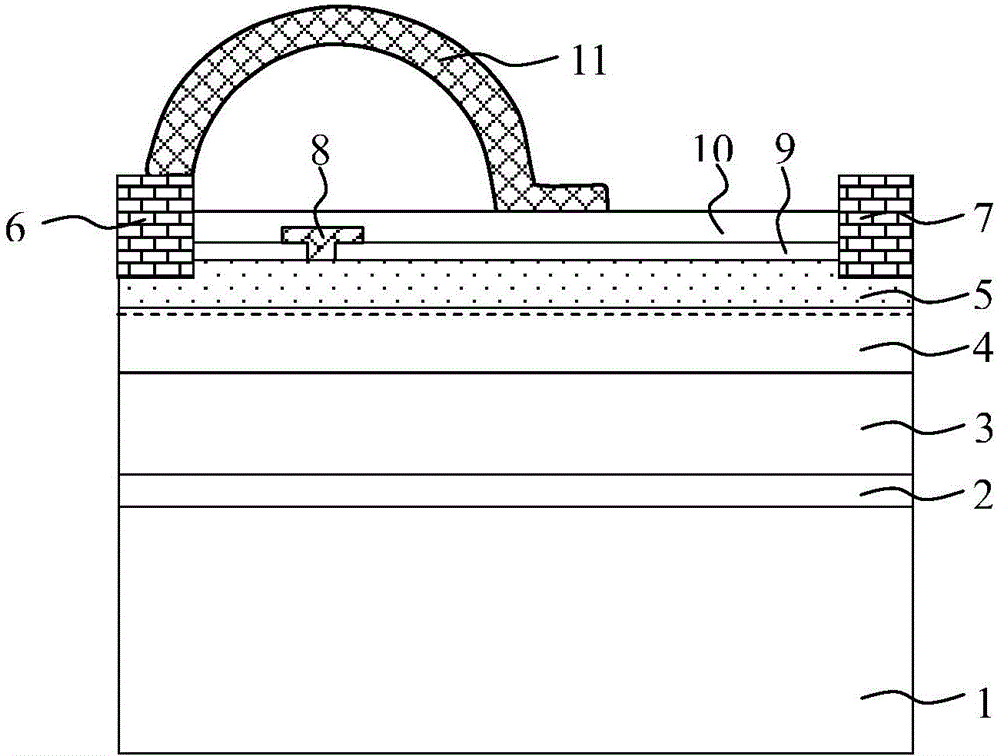
[0063] Figure 3A is a schematic cross-sectional view of a semiconductor device with a segmented air-isolated source-field plate structure in the first embodiment of the present invention, Figure 3B Its plan view.

[0064] like Figure 3A As shown, the semiconductor device includes:

[0065] Substrat...


PUM


Abstract

The invention discloses a semiconductor device and a manufacturing method thereof. The semiconductor device comprises a substrate, a semiconductor layer located on the substrate, a source and a drain located on the semiconductor layer, a gate located between the source and the drain, a source field plate located on the semiconductor layer and connected with the source, wherein the source field plate passes across the gate, the gate/source region and part of the gate/drain region, and air isolation is carried out; one end of the source field plate is connected with the source; two or more than two metal field plates are connected in parallel to form connection between the source field plate and the source; and the other end of the source field plate is located on the semiconductor layer, close to the gate, between the gate and the drain. A role of electric field modulation of the source field plate can be fully played, parasitic gate/source capacitance and parasitic conduction resistance can be fully reduced, and reliability of the device is improved.

Description

technical field [0001] The invention relates to the technical field of semiconductors, in particular to a semiconductor device and a manufacturing method thereof. Background technique [0002] Gallium nitride (GaN) semiconductor material has a relatively large forbidden band width. Based on the heterojunction structure formed by gallium nitride (GaN) semiconductor material, a high-concentration two-dimensional electron gas can be generated at the heterojunction interface and is confined In the quantum well, the electron mobility is very high. Semiconductor devices made using this feature, such as high electron mobility transistors (HEMT), have the characteristics of large breakdown electric field, high current density, and fast electron saturation drift speed, which are very suitable for making high temperature, high frequency, high voltage and high power devices. It can be widely used in the field of radio frequency microwave and power electronics, and is one of the resear...

Claims


Application Information

Patent Timeline
Patent Type & Authority Applications(China)
IPC IPC(8): H01L29/78H01L21/336
CPCH01L29/404H01L29/66462H01L29/7781
Inventor 张乃千裴轶刘飞航
Owner GPOWER SEMICON
Why Eureka
Try Eureka